Introduction: The Quest for Matter That Computes
As I set up a local Large Language Model (LLM) on my laptop last week, I was amazed at the incredible speed improvement compared to running inference on a friend’s five-year-old machine. Yet beneath this remarkable software progress lies an inescapable physical bottleneck: our conventional computing infrastructure is colliding with fundamental thermodynamic and architectural limits.
The question, of course, is how we can advance our understanding of matter to create ever more powerful, energy-efficient computing systems. Two complementary paths lead toward this goal: developing new, more efficient technology stacks or optimizing existing compute resources. Personally, I am drawn to the prospect of etching neural dynamics directly onto physical systems—harnessing the intrinsic non-linearities, topology, and transport phenomena of condensed matter to build neuromorphic and unconventional computing architectures.
Background & Experimental Foundations
My fascination with nanoscale physics and hardware began as an undergraduate in the Solid State Physics Laboratory at BITS Pilani, K.K. Birla Goa Campus, where I worked under Dr. Ram Shanker Patel and Dr. Dhavala Suri, gaining hands-on experience in basic transport measurements and instrument interfacing.
The physics department offered a rich curriculum of fundamental and technologically relevant courses—including Quantum Information and Computation, Analog and Digital VLSI Design, a study-oriented project on Topological Insulators, and Non-linear Dynamics. These courses provided a rigorous theoretical foundation while sparking my curiosity to delve into cutting-edge topics. I followed up by taking dedicated reading courses with faculty on the quantum Hall effect in graphene and 2D materials, topological insulators, and mesoscopic transport. In parallel, coursework in Object-Oriented Programming, Computational Physics, Introduction to High Performance Computing, and computational modeling using Density Functional Theory (DFT) allowed me to bridge experimental physics with scientific computation.
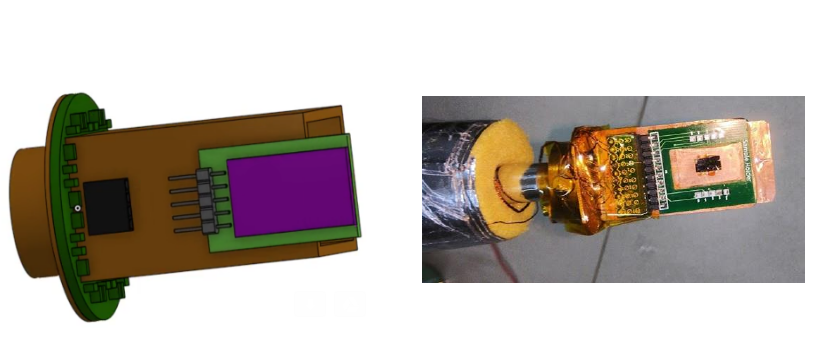
In the summer of my second year, I worked as an intern in the Superconductivity Lab at the National Institute of Science Education and Research (NISER), Bhubaneswar. My project was to design a customized probe for a closed-cycle liquid helium cryostat to perform low-temperature electrical transport measurements. Through this internship, I developed essential practical engineering skills:
- 3D CAD modeling of the probe head to ensure optimal thermal contact with the sample while minimizing the thermal load on the cryostat (using Fusion 360, Onshape, and Blender).
- PCB designing for sample holders and multi-stage RC filtering to suppress high-frequency electrical noise (using Eagle CAD and EasyEDA).
- Automated instrumentation interfacing of source measure units (SMUs) and cryogenic temperature controllers for automated resistance-versus-temperature (\(R\text{–}T\)) measurements using LabVIEW and Python.
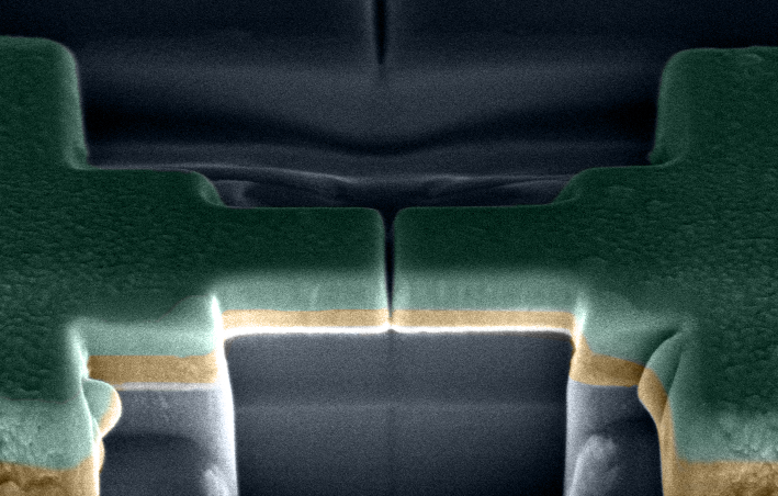
In my final year, as part of my Master’s thesis under Dr. Kartik Senapati at NISER, I worked on a year-long project focused on the fabrication and low-temperature transport characterization of vertical and planar Copper/Niobium (\(\text{Cu/Nb}\)) Josephson junctions. By measuring their \(R\text{–}T\), current-voltage (\(I\text{–}V\)), and voltage-versus-magnetic-field (\(V\text{–}H\)) characteristics, we verified device functionality and probed interfacial spin-orbit coupling phenomena. This work culminated in a co-authored publication in Nature Communications demonstrating the phase biasing of a Josephson junction via the Rashba-Edelstein effect [23].
My experimental work involved cleanroom fabrication and characterization tools, including UV optical lithography, DC magnetron sputtering, scanning electron microscopy (SEM), Gallium-ion Focused Ion Beam (Ga-FIB) milling, and Physical Property Measurement Systems (PPMS).
Holding a dual major in Physics and Electronics & Instrumentation gave me a unique vantage point: understanding the quantum and solid-state physics of materials while being able to rapidly design auxiliary circuitry, build custom data acquisition software, and interface laboratory instruments.
Following my Master’s, I joined the Scientific Support Unit at the Max Planck Institute for the Structure and Dynamics of Matter (MPSD) in Hamburg as a Research Software Engineer. There, I worked on massively parallel scientific software, high-performance computing (HPC) workflows, Monte Carlo simulations using the Wang and Landau algorithm, and reproducible research infrastructure.
It was obvious by then that I was very keen on computing. While I was researching for PhD positions, I kept looking at several kinds of computing paradigms that keep popping up. And the following is a small list of types of computing systems I’ve come across. It is indeed interesting to see how we name nature in different levels to make it do what we want it to do.
In this article, I reflect on the principles and physical trajectories underpinning this transition. We will explore:
-
The physical imperative for neuromorphic architectures: Why modern AI demands a departure from the Von Neumann paradigm, and what physical principles make biological brains orders of magnitude more efficient.
-
Physical implementation trajectories: From quantum materials and tunable resistive devices (memristors) to topological spin textures (magnetic and electric skyrmions).
-
Stochastic and Brownian computing: Utilizing thermal fluctuations, skyrmion reshufflers, and token-based Brownian half-adders to perform non-arithmetic and near-zero-energy computations.
-
Physical reservoir computing: Exploiting the high-dimensional, non-linear dynamics of magnetic textures and ferroelectric domain walls to process temporal and spatial data without iterative backpropagation.
-
Analog crossbar arrays & Ferroelectric Hafnia (\(\text{HfO}_2\)): Performing \(O(1)\) parallel vector-matrix multiplication in the analog domain, the crystallographic polymorphism of ferroelectric hafnia thin films, and the experimental techniques needed to engineer nanoscale synaptic devices.
Unconventional Computing: The Physical Need
The Thermodynamic Wall of Deep Learning
The ongoing revolution in machine learning and artificial intelligence revolves around processing unprecedented volumes of data. Image recognition, natural language translation, audio processing, and generative modeling excel at finding structure in massive datasets. However, executing even an elementary image classification task—such as distinguishing a cat from a dog—consumes hundreds of watts on contemporary graphics processing units (GPUs). In stark contrast, the human biological brain performs this task almost instantaneously while drawing a total power budget of approximately 10 to 20 Watts [13].
This orders-of-magnitude disparity in energy efficiency is a fundamental thermodynamic challenge. As global computation demands scale exponentially, electricity consumption and its associated carbon footprint become critical constraints. To transcend this efficiency wall, we must look beyond standard synchronous digital logic and draw inspiration from the computational principles of the biological nervous system.
The extraordinary energy efficiency of biological brains stems from several key architectural and physical properties [13]:
-
Sparse Signaling & Noise Tolerance: Unlike continuous, high-frequency digital clocking, biological neurons communicate via intermittent, asynchronous action potentials (spikes). Information is encoded sparsely in time and space, enabling the system to operate at minimal dynamic power while naturally tolerating stochastic thermal noise.
-
Co-located Memory and Processing: Biological neurons and synapses simultaneously store information and compute with it. This completely eliminates the classical Von Neumann bottleneck—the costly, energy-intensive movement of data back and forth between physically separated CPU/GPU logic and DRAM memory buses.
-
Massive Parallelism: The brain employs vast parallel connectivity across approximately \(10^{11}\) neurons and \(10^{14}\) synapses, achieving immense aggregate computational throughput despite low operational speeds (~10–100 Hz).
-
Adaptive, Plastic Synapses: Biological synapses dynamically adjust their connection strengths (weights) via local biochemical and biophysical mechanisms (such as Spike-Timing-Dependent Plasticity, STDP), enabling continuous on-line learning without global backpropagation.
-
Inherent Fault Tolerance: The brain functions robustly despite the stochastic death or failure of individual neurons due to redundant connectivity and continuous structural plasticity.
-
Stochasticity as a Feature: Thermal noise and probabilistic ion-channel gating provide an intrinsic source of randomness that facilitates probabilistic inference, sampling, and escape from local energetic minima.
By embedding these physical principles directly into solid-state hardware, neuromorphic engineering aims to create non-Von Neumann processors capable of learning and inferring at biological efficiency levels. While initial silicon implementations like IBM’s TrueNorth and Heidelberg’s BrainScaleS demonstrated the viability of brain-inspired spike routing, realizing the full potential of neuromorphic computing requires nanoscale materials that inherently compute through their internal physics.
Trajectories for Physical Hardware Implementation
Quantum Materials and Non-Linear Dynamics
Quantum materials exhibit rich, highly non-linear responses to modest external stimuli [10]. Abrupt changes in electrical resistivity, optical transmission, or magnetic order can be triggered by small electrical voltages, thermal gradients, or optical pulses. In conventional transistors, non-linearity must be engineered through steep subthreshold gate electrostatics. In quantum materials, non-linearity is an intrinsic property of strongly correlated electrons, enabling artificial neurons and synapses with orders-of-magnitude smaller footprints and lower switching energies.
1. Tunable Resistive Devices: Memristors and Phase Change Materials
Memristors—two-terminal passive components whose resistance depends on the history of electric charge or voltage applied across them—are prime candidates for artificial electronic synapses [11], [19], [25], [28]. Their non-volatile, continuously tunable resistance states mimic synaptic weight modulation.
Memristive switching relies on several distinct physical mechanisms [26], [27]:
- Electrochemical Metallization (ECM): The voltage-driven migration of active metal cations (such as \(\text{Ag}^+\) or \(\text{Cu}^{2+}\)) through an insulating matrix to form and rupture metallic conductive filaments.
- Valence Change Mechanisms (VCM): The drift and diffusion of oxygen vacancies in transition metal oxides (\(\text{TiO}_{2-x}\), \(\text{HfO}_{2-x}\), \(\text{TaO}_{x}\)), modulating local Schottky or tunneling barriers.
- Phase Change Materials (PCM): Reversible structural transitions between a high-conductance crystalline state and a low-conductance amorphous state, typically in chalcogenide alloys like \(\text{Ge}_2\text{Sb}_2\text{Te}_5\) (GST). While PCMs offer mature fabrication, their switching requires substantial Joule heating to melt the material, and continuous bidirectional analog tuning can be limited by resistance drift and asymmetric crystallization dynamics.
Advanced memristive devices exhibit device footprints below 10 nm, data retention spanning decades, sub-nanosecond switching speeds, high cycling endurance (\(>10^9\) cycles), and operational currents in the nanoampere to picoampere regime. When organized into 2D crossbar matrices, they execute parallel vector-matrix multiplication directly at the site of data storage [21].
Topological Spin Structures for Computation
Beyond electronic charge transport, the electron’s spin degree of freedom offers dissipation-suppressed pathways for computing. In magnetic thin films with broken inversion symmetry, the interfacial Dzyaloshinskii-Moriya Interaction (DMI) stabilizes topologically protected spin configurations known as magnetic skyrmions [7].
Skyrmions are nanoscale vortex-like whirls of magnetization characterized by an integer topological winding number:
Because \(N_{\text{sk}} \in \mathbb{Z}\), a skyrmion cannot be smoothly deformed into a uniform ferromagnetic ground state without creating an energetic singularity. This topological protection makes skyrmions exceptionally robust against structural defects and thermal fluctuations. Furthermore, skyrmions can be set into motion by spin-polarized electrical currents via spin-orbit torques (SOT) at current densities several orders of magnitude lower than those required to drive conventional ferromagnetic domain walls.
More recently, analogous topologically protected configurations of electric dipoles—such as polar skyrmions, merons, and hopfions—have been discovered in ferroelectric oxide superlattices (such as \((\text{SrTiO}_3)_n / (\text{PbTiO}_3)_n\)) [6]. These polar textures couple directly to electric fields rather than magnetic fields, holding immense promise for ultra-low-energy voltage-controlled neuromorphic devices that eliminate the inductive and resistive penalties of current-driven spintronics. Crucially, as we will discuss in Section 5, ferroelectric oxides based on doped \(\text{HfO}_2\) can be seamlessly integrated into standard CMOS Back-End-of-Line (BEOL) fabrication processes [22].
Stochastic & Brownian Computing
Skyrmion Reshufflers for Probabilistic Computing
Conventional digital computers treat thermal fluctuations as unwanted noise that must be suppressed by maintaining high voltage margins. Stochastic computing, by contrast, embraces randomness by representing numbers as probabilistic bit streams [17]. For example, a real number \(p \in [0, 1]\) is represented by a sequence of random binary bits where the probability of observing a '1' equals \(p\).
In this probabilistic representation, complex mathematical operations collapse into elementary logic:
- Multiplying two independent stochastic bit streams \(A\) (probability \(p_A\)) and \(B\) (probability \(p_B\)) is performed using a single AND gate, since \(P(A \land B) = p_A \times p_B\).
- Scaled addition can be performed using an elementary multiplexer.
However, the mathematical validity of stochastic computing requires the bit streams to be strictly uncorrelated. Generating truly random, uncorrelated bit streams using conventional pseudo-random number generators (LFSRs) requires substantial silicon area and energy.
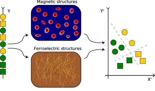
Nanoscale skyrmions provide a natural physical solution. Due to their particle-like nature and low pinning thresholds at room temperature, skyrmions exhibit pronounced Brownian thermal diffusion. Zázvorka et al. [29] demonstrated a physical skyrmion reshuffler device: thermal excitation randomizes the spatial order of skyrmion tokens moving through a microfluidic-like magnetic chamber while preserving the overall token density (probability). This device achieved a residual correlation of only 11%, demonstrating that nanoscale spin textures can serve as native entropy sources for probabilistic computation.
Token-Based Brownian Computing
Taking thermodynamic efficiency to its ultimate limit, Brownian computing operates near the fundamental Landauer limit (\(k_B T \ln 2\) per bit erasure) by allowing thermal fluctuations to drive the computation forward and backward through a state space [14].
In token-based Brownian circuits, discrete physical particles (such as individual skyrmions) act as computational tokens. Computation is mediated by three fundamental geometric building blocks [14]:
- Hubs: Junctions that allow tokens to diffuse between interconnected tracks.
- Ratchets: Asymmetric potential barriers that establish a preferred drift direction under thermal excitation, preventing backward diffusion.
- C-Joints (Conservative Coincidence Gates): Non-linear junctions where two tokens must arrive simultaneously to interact and exit through designated output channels.
These components have been experimentally verified in continuous magnetic thin films [1], [12]. For instance, research teams have demonstrated a skyrmion-based Brownian half-adder: two input skyrmions diffuse into a central C-joint region; if both are present, their mutual repulsive interaction steers them into the ‘Carry’ output track, whereas a single token exits along the ‘Sum’ track. Computation proceeds via thermal diffusion, requiring minimal external energy input.
Physical Reservoir Computing
Architectural Principles of Reservoir Computing
Recurrent Neural Networks (RNNs) are powerful tools for processing temporal, sequential, and dynamical data (such as time-series forecasting, speech recognition, and non-linear system identification). However, training standard RNNs requires Backpropagation Through Time (BPTT)—an algorithm that is computationally demanding, prone to vanishing and exploding gradients, and difficult to implement directly on edge hardware.
Reservoir Computing (RC) bypasses the training of recurrent weights entirely [7]. The architecture consists of three distinct stages:
- Input Layer: Feeds the external temporal signal \(\mathbf{u}(t)\) into the reservoir.
- The Reservoir: A complex, fixed, non-linear recurrent network that projects the low-dimensional input into a high-dimensional spatiotemporal state space \(\mathbf{x}(t)\).
- Readout Layer: A simple linear layer that maps the reservoir states to the target output \(\mathbf{y}(t) = \mathbf{W}_{\text{out}} \mathbf{x}(t)\).
Crucially, the internal connections of the reservoir are never modified during training. Only the weights of the linear readout layer (\(\mathbf{W}_{\text{out}}\)) are trained, which can be accomplished using simple, closed-form linear regression (such as ridge regression or pseudo-inverse methods):
This eliminates iterative gradient descent through the recurrent core, making reservoir computing fast to train and ideally suited for physical hardware implementations.
Core Requirements for a Physical Reservoir:
- High Dimensionality: The physical substrate must map low-dimensional input signals into a vast space of non-linearly coupled physical observables.
- Non-linearity: The system’s response to driving forces must be non-linear to render linearly inseparable problems separable in reservoir state space (Figure 2a).
- Short-Term (Fading) Memory: The current physical state must retain information about past inputs over a finite time window (the echo state property), with past influence decaying smoothly to zero.
- Reproducibility: Identical input driving sequences must produce identical reservoir trajectories across experimental runs.
Emulating these properties on digital transistors requires substantial circuitry. In contrast, condensed matter systems inherently exhibit non-linearity, memory, and complex collective dynamics at the nanometer scale.
Magnetic Systems for Reservoir Computing
Magnetic materials are exceptional candidates for physical reservoirs because their spin configurations respond non-linearly to magnetic fields, electrical currents, mechanical strain, and light [7]. Furthermore, magnetic devices can be integrated with CMOS circuitry via magnetic tunnel junction (MTJ) technology.
Candidate magnetic reservoir platforms include:
- Dipole-Coupled Nanomagnet Arrays: Lithographically patterned islands of ferromagnets whose stray dipolar fields create complex collective relaxation dynamics.
- Spin-Wave Reservoirs: Propagating magnons in yttrium iron garnet (YIG) thin films whose non-linear interference processes temporal microwave signals.
- Skyrmion Fabrics: Dense, disordered ensembles of magnetic skyrmions confined in thin-film geometries [2], [18], [20].
When an electrical voltage pulse train is applied across a skyrmion fabric, the resulting current exerts spin-transfer and spin-orbit torques on the skyrmions. The textures deform, compress, and interact with material pinning sites. The competition between pinning forces, internal elasticity, and driving torques produces reproducible non-linear deformation and fading memory [18], [20]. As the current ceases, the magnetic fabric relaxes toward an energetic equilibrium, encoding historical pulse sequences into the local anisotropic magnetoresistance (AMR) or topological Hall voltage. Extending these magnetic textures into the third spatial dimension (3D vertical nanowires and multilayered stacks) further magnifies the available state space [18].
Ferroelectric Systems for Reservoir Computing
Complementing spin-based reservoirs, ferroelectric materials provide an electrical-field-driven alternative that eliminates Ohmic Joule losses associated with steady-state currents [7].
In ferroelectrics, the spontaneous electric polarization can be reoriented by external electric fields, mechanical stress, or optical illumination, producing rich hysteretic and non-linear responses. Diverse device architectures have been explored:
- Ferroelectric Tunnel Junctions (FTJs): Nanometer-thin ferroelectric barriers sandwiched between metal electrodes, where polarization reversal modulates the quantum mechanical tunneling electroresistance (TER).
- Ferroelectric Field-Effect Transistors (FeFETs): Where a ferroelectric gate dielectric modulates the channel conductance of a semiconductor [8], [15].
- Conductive Ferroelectric Domain Walls: The interface separating adjacent domains of differing polarization direction [16], [21].
Ferroelectric domain walls are especially compelling. While the surrounding bulk domains are insulating dielectrics, the domain walls can exhibit substantial electrical conductivity due to localized band bending, structural distortions, and oxygen vacancy accumulation.
When external voltage pulses are applied, these domain walls move, bend, and nucleate, altering their geometric length and connectivity. This dynamic reconfiguration yields non-linear conductance modulation with intrinsic fading memory [7]. Because domain wall dynamics depend on local defect pinning and elastic restoring forces, networks of domain walls act as physical reservoirs where input voltage signals are naturally mapped into complex conductance states across multi-terminal electrode arrays [21].
Analog Crossbar Arrays & Ferroelectric Hafnia
The Crossbar Array Architecture
Deep neural networks execute trillions of multiply-accumulate (MAC) operations:
On conventional digital GPUs, evaluating this matrix-vector multiplication scales with computational complexity \(O(n^2)\). Each weight must be fetched from memory, loaded into registers, processed in floating-point arithmetic logic units (ALUs), and written back. Memory bus bandwidth and capacitive charging of long interconnect lines dominate system energy consumption.
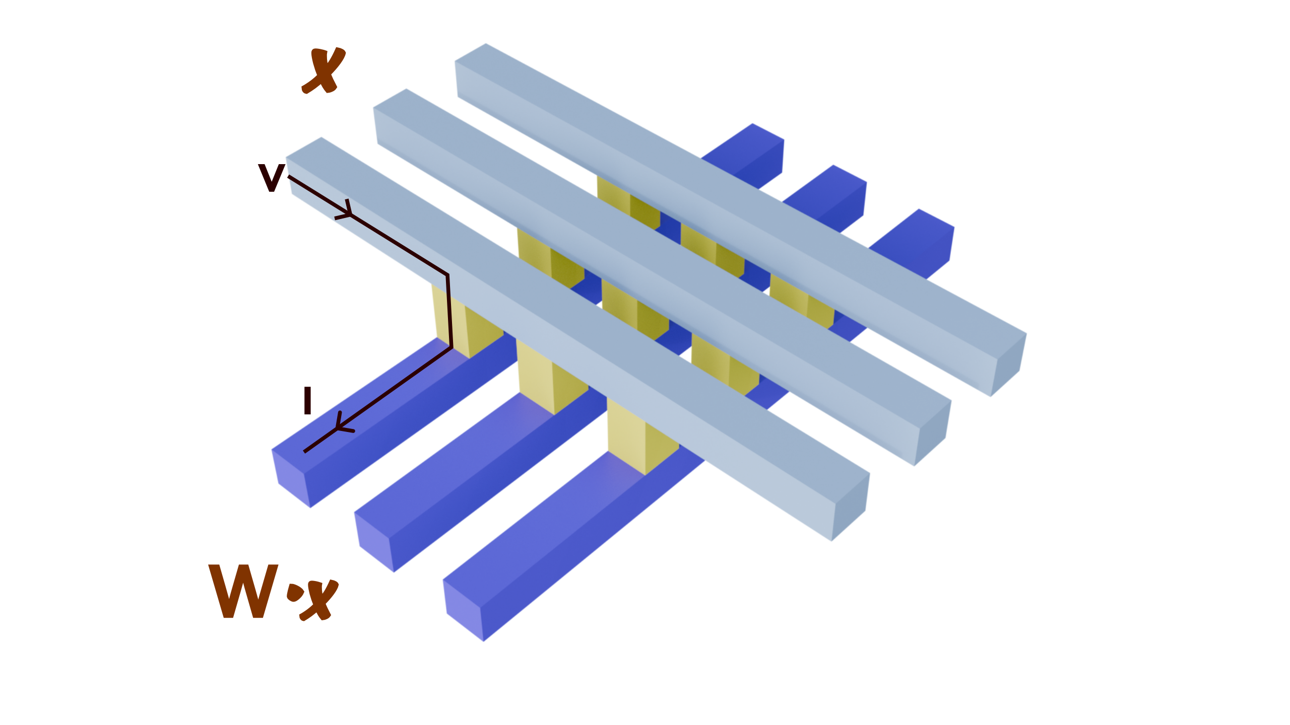
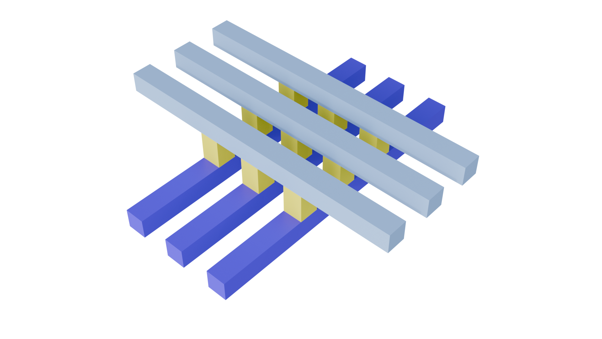
Analog crossbar arrays circumvent this bottleneck by performing matrix-vector multiplication in a single physical step using the fundamental laws of electrical circuits:
-
Ohm’s Law: When an input voltage \(V_i\) is applied across a two-terminal device with conductance \(G_{ji}\), the resulting current is:
$$I_{ji} = V_i \cdot G_{ji}$$ -
Kirchhoff’s Current Law (KCL): When multiple rows feed into a common column line, the currents sum algebraically at the node:
$$I_j = \sum_{i=1}^n I_{ji} = \sum_{i=1}^n V_i \cdot G_{ji}$$
By mapping neural network inputs to row voltages \(\mathbf{V}\), synaptic weights to junction conductances \(\mathbf{G}\), and reading out the column currents \(\mathbf{I}\), the entire matrix-vector product is computed in \(O(1)\) time complexity in the analog domain [3].
Synaptic Device Requirements
To realize high-precision analog acceleration, the crosspoint synaptic device must satisfy stringent physical criteria:
- Fine, Continuous Conductance Tuning: The device must support numerous distinct, stable conductance levels (ideally \(>1000\) levels) under identical programming pulses to enable high weight resolution.
- High Dynamic Resistance Range: Overall device resistance should reside in the \(1\text{ to }100\text{ M}\Omega\) regime. Low-resistance devices draw excessive current, causing parasitic \(IR\) voltage drops along metallic interconnect lines that degrade computational accuracy.
- Bidirectional Symmetry & Linearity: Weight potentiation (conductance increase) and depression (conductance decrease) should exhibit linear, symmetric trajectories.
- CMOS Compatibility: The materials must be synthesizable within the thermal and contamination constraints of standard silicon manufacturing (Back-End-of-Line, BEOL).
Traditional candidates like phase-change materials (PCMs) and valence-change metal oxides (\(\text{TiO}_x\), \(\text{TaO}_x\)) often struggle with non-linear switching, high programming currents, and resistance drift. Consequently, attention has converged on ferroelectric hafnium oxide (\(\text{HfO}_2\)) memristive devices with engineered electrodes (such as \(\text{WO}_{3-x}\)), which demonstrate reversible analog resistance modulation, sub-nanosecond switching dynamics, and exceptional BEOL integration potential [4], [8].
Material Physics of Ferroelectric Hafnia (\(\text{HfO}_2\))
The 2011 Paradigm Shift
For decades, ferroelectricity was believed to be restricted to complex perovskite oxides (such as \(\text{BaTiO}_3\) and \(\text{Pb}(\text{Zr,Ti})\text{O}_3\)). These materials suffer from severe scaling limitations: when scaled below ~10 nm, depolarizing fields suppress ferroelectricity (the “critical thickness problem”). Furthermore, perovskite materials contain incompatible elements (lead, bismuth) that poison standard silicon fabrication lines.
In 2011, Böscke et al. reported the breakthrough discovery of robust ferroelectricity in silicon-doped hafnium oxide (\(\text{Si:HfO}_2\)) thin films capped with TiN electrodes [5]. This was an astonishing finding: \(\text{HfO}_2\) was already the standard high-\(k\) dielectric used in commercial CMOS transistor gates (introduced at the 45 nm node). Worldwide research over the subsequent decade confirmed that nanoscale doped \(\text{HfO}_2\) thin films retain robust polarization down to thicknesses below 5 nm [24].
Zirconium has emerged as the preferred dopant (\(\text{Hf}_{0.5}\text{Zr}_{0.5}\text{O}_2\), HZO) because \(\text{HfO}_2\) and \(\text{ZrO}_2\) form a continuous solid solution with lower crystallization temperatures (~\(400^\circ\text{C}\)), fully compatible with BEOL thermal budgets.
Multifunctional Properties of Ferroelectric Hafnia
Ferroelectric \(\text{HfO}_2\) exhibits a versatile spectrum of physical properties [24]:
- Pyroelectricity: Generates electrical charge in response to temperature variations, opening pathways for integrated infrared and thermal gas sensors.
- Piezoelectricity: Converts mechanical strain into electrical voltage and vice versa, enabling integrated nano-electromechanical systems (NEMS), acoustic resonators, and energy harvesters.
- Tunable Non-Volatile Polarization: Enables diverse electronic device classes:
- Ferroelectric Random Access Memories (FeRAMs): Ultra-fast, low-power capacitive bit cells.
- Ferroelectric Field-Effect Transistors (FeFETs): Three-terminal devices where gate polarization modulates semiconductor channel conductance [15].
- Ferroelectric Tunnel Junctions (FTJs): Two-terminal devices where spontaneous polarization modulates quantum mechanical tunneling electroresistance, delivering power-efficient non-volatile analog memristive switching.
Polymorphic Crystalline Phases
The origin of ferroelectricity in \(\text{HfO}_2\) lies in a metastable, non-centrosymmetric orthorhombic crystalline phase. Pure bulk \(\text{HfO}_2\) is not ferroelectric at ambient conditions. Instead, thin films exhibit rich polymorphism among several competing phases [22], [24]:
| Crystalline Phase | Space Group | Centrosymmetric? | Polar / Ferroelectric? | Physical Description & Stability |
|---|---|---|---|---|
| Monoclinic (\(m\)) | \(P2_1/c\) | Yes | No (Dielectric) | Thermodynamically stable ground state at room temperature. Exhibits a low dielectric constant (\(k \approx 16\text{–}20\)). Detrimental to ferroelectric device performance. |
| Cubic (\(c\)) | \(Fm\bar{3}m\) | Yes | No (Dielectric) | Stable at high temperatures (\(>2500^\circ\text{C}\)) or high dopant concentrations. Characterized by high dielectric constant (\(k \approx 30\text{–}40\)). |
| Tetragonal (\(t\)) | \(P4_2/nmc\) | Yes | No (Antiferroelectric-like) | High-temperature phase (\(>1700^\circ\text{C}\)). Antiferroelectric-like behavior with field-induced transition to polar phase. High dielectric constant. |
| Orthorhombic (\(o\text{-FE}\)) | \(Pca2_1\) | No | Yes (Ferroelectric) | Metastable polar phase. Arises from a non-centrosymmetric displacement of oxygen atoms along the polar \(c\)-axis. Stabilized by nanoscale grain boundaries, mechanical clamping, chemical doping, and oxygen vacancies. |
Because the polar orthorhombic phase (\(Pca2_1\)) is metastable relative to the non-polar monoclinic ground state (\(P2_1/c\)), stabilizing it requires careful optimization of several thermodynamic and kinetic parameters:
-
Surface Energy & Grain Size: Due to lower surface energy of the orthorhombic/tetragonal phases compared to the monoclinic phase, keeping grain sizes small (below ~10 nm) thermodynamically stabilizes the polar phase.
-
Chemical Doping: Doping with \(\text{Zr}^{4+}\), \(\text{Si}^{4+}\), \(\text{Al}^{3+}\), \(\text{Y}^{3+}\), or \(\text{La}^{3+}\) induces internal lattice strain and promotes oxygen vacancy formation that inhibits transformation into the monoclinic phase.
-
Electrode Clamping: Capping with top and bottom metallic electrodes (such as TiN or TaN) provides mechanical confinement and in-plane tensile stress during Rapid Thermal Annealing (RTA), freezing in the non-centrosymmetric orthorhombic lattice.
Experimental & Device Engineering Roadmap
To translate ferroelectric \(\text{HfO}_2\) into functional analog crossbar computing arrays, several experimental frontiers are being actively pursued:
-
Atomic Layer Deposition (ALD): Thin films must be grown with sub-angstrom thickness control and atomic stoichiometry. ALD using metal-organic precursors (such as TDMA-Hf, TDMA-Zr) and oxidizers (\(\text{H}_2\text{O}\) or \(\text{O}_3\)) allows conformal deposition on high-aspect-ratio 3D structures.
-
Nanostructural Characterization (HR-TEM): High-Resolution Transmission Electron Microscopy coupled with energy-dispersive X-ray spectroscopy (EDX) is critical to elucidate polycrystalline grain boundaries, phase segregation, and interdiffusion at the \(\text{TiN/HfO}_2\) interface.
-
Piezoresponse Force Microscopy (PFM): PFM enables real-space visualization of nanoscale domain switching dynamics, domain wall velocity, and local coercive field distributions under applied tip biases.
-
Ultrafast Pulse Manipulation: Exploring the manipulation of hafnia’s crystalline microstructure via ultrafast sub-nanosecond electric pulses. Short, intense pulses induce controlled local Joule heating to amorphize or de-crystallize the material, followed by large adiabatic relaxation pulses to re-crystallize it into desired polymorphic phase distributions.
-
Multiphysics Tuning: Investigating the interplay of mechanical strain, local temperature gradients, and optical excitation as external tuning parameters to dynamically modulate synaptic conductance.
-
FeFET Synaptic Integration: Implementing ferroelectric Field-Effect Transistors as synaptic elements [8], [15], where partial polarization switching of the gate oxide provides multi-level non-volatile channel conductance states with minimal read disturb.
Summary & Outlook
The transition toward unconventional and neuromorphic computing represents one of the most intellectually invigorating frontiers in condensed matter physics and computer engineering. As standard silicon scaling hits thermal, interconnect, and memory-bandwidth limits, progress hinges on exploiting the intrinsic physics of matter to perform computation.
Whether through:
- the topological stability and Brownian diffusion of magnetic skyrmions for stochastic computing,
- the high-dimensional fading-memory dynamics of magnetic fabrics and ferroelectric domain walls in physical reservoir computing, or
- the parallel \(O(1)\) vector-matrix multiplication of CMOS-compatible ferroelectric hafnium oxide analog crossbar arrays,
the future of computing lies at the interface of nanoscale material physics, experimental instrumentation, and brain-inspired architectures. Bridging the gap between fundamental laboratory discoveries and scalable solid-state devices will shape the next era of energy-efficient, cognitive hardware.
References
[1] M. Goto, R. Ishikawa, S. Miki, T. Nozaki, Y. Suzuki, and E. Tamura, “GA-03: Hidden skyrmion diffusion and Brownian computing,” IEEE INTERMAG Conference, 2021.
[2] G. Bourianoff, D. Pinna, M. Sitte, and K. Everschor-Sitte, “Potential implementation of reservoir computing models based on magnetic skyrmions,” AIP Advances, vol. 8, no. 5, p. 055602, 2018. doi:10.1063/1.5006918
[3] L. Bégon-Lours, M. Halter, D. Dávila Pineda, V. Bragaglia, Y. Popoff, A. La Porta, D. Jubin, J. Fompeyrine, and B. J. Offrein, “A Back-End-Of-Line Compatible, Ferroelectric Analog Non-Volatile Memory,” 2021 IEEE International Memory Workshop (IMW), pp. 1–4, 2021. doi:10.1109/IMW51353.2021.9439600
[4] L. Bégon-Lours, M. Halter, Y. Popoff, Z. Yu, D. F. Falcone, D. Dávila, V. Bragaglia, A. La Porta, D. Jubin, J. Fompeyrine, and B. J. Offrein, “Analog Resistive Switching in BEOL, Ferroelectric Synaptic Weights,” IEEE Journal of the Electron Devices Society, vol. 9, pp. 1275–1281, 2021. doi:10.1109/JEDS.2021.3129598
[5] T. S. Böscke, J. Müller, D. Bräuhaus, U. Schröder, and U. Böttger, “Ferroelectricity in hafnium oxide thin films,” Applied Physics Letters, vol. 99, no. 10, p. 102903, 2011. doi:10.1063/1.3634052
[6] S. Das, Y. L. Tang, Z. Hong, M. A. P. Gonçalves, M. R. McCarter, C. Klewe, K. X. Nguyen, F. Gómez-Ortiz, P. Shafer, E. Arenholz, V. A. Stoica, S.-L. Hsu, B. Wang, C. Ophus, J. F. Liu, C. T. Nelson, S. Saremi, B. Prasad, A. B. Mei, D. G. Schlom, J. Íñiguez, P. García-Fernández, D. A. Muller, L. Q. Chen, J. Junquera, L. W. Martin, and R. Ramesh, “Observation of room-temperature polar skyrmions,” Nature, vol. 568, no. 7752, pp. 368–372, 2019. doi:10.1038/s41586-019-1092-8
[7] K. Everschor-Sitte, A. Majumdar, K. Wolk, and D. Meier, “Novel implementations for reservoir computing – from spin to charge,” arXiv preprint arXiv:2311.12185, 2023.
[8] D. F. Falcone, M. Halter, L. Bégon-Lours, and B. J. Offrein, “Back-End, CMOS-Compatible Ferroelectric FinFET for Synaptic Weights,” Frontiers in Electronic Materials, vol. 2, p. 883196, 2022. doi:10.3389/femat.2022.883196
[9] H. Fangohr et al., “Ground state search, hysteretic behaviour and reversal mechanism of skyrmionic textures in confined helimagnetic nanostructures,” Scientific Reports, vol. 5, no. 1, p. 17300, 2015. doi:10.1038/srep17300
[10] A. Hoffmann et al., “Quantum materials for energy-efficient neuromorphic computing: Opportunities and challenges,” APL Materials, vol. 10, no. 7, p. 070904, 2022. doi:10.1063/5.0094205
[11] D. Ielmini and H.-S. P. Wong, “In-memory computing with resistive switching devices,” Nature Electronics, vol. 1, no. 6, pp. 333–343, 2018. doi:10.1038/s41928-018-0092-2
[12] Y. Jibiki et al., “Skyrmion Brownian circuit implemented in continuous ferromagnetic thin film,” Applied Physics Letters, vol. 117, no. 8, p. 082402, 2020. doi:10.1063/5.0019918
[13] D. Kuzum, R. G. D. Jeyasingh, B. Lee, and H.-S. P. Wong, “Nanoelectronic Programmable Synapses Based on Phase Change Materials for Brain-Inspired Computing,” Nano Letters, vol. 12, no. 5, pp. 2179–2186, 2011. doi:10.1021/nl201040y
[14] J. Lee et al., “Brownian Circuits: Designs,” International Journal of Unconventional Computing, vol. 12, pp. 341–362, 2016.
[15] H. Mulaosmanovic, J. Ocker, S. Müller, M. Noack, J. Müller, P. Polakowski, T. Mikolajick, and S. Slesazeck, “Novel ferroelectric FET based synapse for neuromorphic systems,” 2017 Symposium on VLSI Technology, pp. T176–T177, 2017. doi:10.23919/VLSIT.2017.7998165
[16] G. F. Nataf, M. Guennou, J. M. Gregg, D. Meier, J. Hlinka, E. K. H. Salje, and J. Kreisel, “Domain-wall engineering and topological defects in ferroelectric and ferroelastic materials,” Nature Reviews Physics, vol. 2, no. 11, pp. 634–648, 2020. doi:10.1038/s42254-020-0235-z
[17] D. Pinna, F. Abreu Araujo, J.-V. Kim, V. Cros, D. Querlioz, P. Bessiere, J. Droulez, and J. Grollier, “Skyrmion Gas Manipulation for Probabilistic Computing,” Physical Review Applied, vol. 9, no. 6, p. 064018, 2018. doi:10.1103/PhysRevApplied.9.064018
[18] D. Pinna, G. Bourianoff, and K. Everschor-Sitte, “Reservoir Computing with Random Skyrmion Textures,” Physical Review Applied, vol. 14, no. 5, p. 054020, 2020. doi:10.1103/PhysRevApplied.14.054020
[19] M. Prezioso, F. Merrikh-Bayat, B. D. Hoskins, G. C. Adam, K. K. Likharev, and D. B. Strukov, “Training and operation of an integrated neuromorphic network based on metal-oxide memristors,” Nature, vol. 521, no. 7550, pp. 61–64, 2015. doi:10.1038/nature14441
[20] D. Prychynenko, M. Sitte, K. Litzius, B. Krüger, G. Bourianoff, M. Kläui, J. Sinova, and K. Everschor-Sitte, “Magnetic Skyrmion as a Nonlinear Resistive Element: A Potential Building Block for Reservoir Computing,” Physical Review Applied, vol. 9, no. 1, p. 014034, 2018. doi:10.1103/PhysRevApplied.9.014034
[21] J. L. Rieck, D. Cipollini, M. Salverda, C. P. Quinteros, L. R. B. Schomaker, and B. Noheda, “Ferroelastic Domain Walls in BiFeO3 as Memristive Networks,” Advanced Intelligent Systems, vol. 5, no. 1, p. 2200230, 2022. doi:10.1002/aisy.202200230
[22] U. Schroeder et al., “Hafnium Oxide Based CMOS Compatible Ferroelectric Materials,” ECS Journal of Solid State Science and Technology, vol. 2, no. 4, pp. N69–N72, 2013. doi:10.1149/2.010304jss
[23] T. Senapati, A. K. Karnad, and K. Senapati, “Phase biasing of a Josephson junction using Rashba Edelstein effect,” Nature Communications, vol. 14, no. 1, p. 7511, 2023. doi:10.1038/s41467-023-43358-0
[24] J. P. B. Silva, L. Bégon-Lours, et al., “Roadmap on ferroelectric hafnia- and zirconia-based materials and devices,” APL Materials, vol. 11, no. 8, p. 089201, 2023. doi:10.1063/5.0148068
[25] D. B. Strukov, G. S. Snider, D. R. Stewart, and R. S. Williams, “The missing memristor found,” Nature, vol. 453, no. 7191, pp. 80–83, 2008. doi:10.1038/nature06932
[26] R. Waser, R. Dittmann, G. Staikov, and K. Szot, “Redox-Based Resistive Switching Memories – Nanoionic Mechanisms, Prospects, and Challenges,” Advanced Materials, vol. 21, no. 25–26, pp. 2632–2663, 2009. doi:10.1002/adma.200900375
[27] M. A. Zidan, A. Chen, G. Indiveri, and W. D. Lu, “Memristive computing devices and applications,” Journal of Electroceramics, vol. 39, no. 1–4, pp. 4–20, 2017. doi:10.1007/s10832-017-0087-4
[28] M. A. Zidan, J. P. Strachan, and W. D. Lu, “The future of electronics based on memristive systems,” Nature Electronics, vol. 1, no. 1, pp. 22–29, 2018. doi:10.1038/s41928-017-0006-8
[29] J. Zázvorka, F. Jakobs, D. Heinze, N. Keil, S. Kromin, S. Jaiswal, K. Litzius, G. Jakob, P. Virnau, D. Pinna, K. Everschor-Sitte, L. Rózsa, A. Donges, U. Nowak, and M. Kläui, “Thermal skyrmion diffusion used in a reshuffler device,” Nature Nanotechnology, vol. 14, no. 7, pp. 658–661, 2019. doi:10.1038/s41565-019-0436-8