Introduction
This article is an adaptation of my Masters thesis report ( first semesters ), where I worked on the fabrications of Josephson Junctions and their charecterisation. In the next article ( second semesters ) I will be talking about modelling the Josephson Junctions computationally and the results obtained from the simulations. At the beginning of this thesis, we introduce basic theoretical concepts that underlay the device we are trying to study, i.e. the Josephson Junction (JJ). We first study the postulates of superconductivity. Then we look at the Josephson effect, which describes the physics of a Superconductor-Insulator-Superconductor sandwich and then look at a popular model of a realistic Josephson junction, namely the RCSJ model. Later we will try to understand various aspects of fabrication and characterisation of such devices.
Superconductivity
Heike Kamerlingh Onnes discovered the phenomenon of superconductivity in the Netherlands in 1911. He was the first to observe that the electrical resistance becomes exactly zero in certain materials and in temperatures below a specific critical value \(T_{c}\) (Schrieffer and Tinkham 1999). Soon after this discovery, several other materials that showed superconducting behaviour were discovered, with different critical temperatures. Currently the highest temperature at which superconductivity was observed is in hydrogen sulphide (\(H_{2}S\)), which has a \(T_{c}\) reported as 203K, but at extremely high pressures (Drozdov et al. 2015). In 1933, Meissner and Ochsenfeld discovered that within a superconductor, the magnetic field completely vanishes i.r becomes zero, making the superconductor a perfect diamagnet. The expulsion of a magnetic field inside a superconductor is called the Meissner effect. Then the London brothers explained this effect, who proved that the magnetic field inside a superconductor has an exponential decay from the surface, with a decay length \(\lambda\), called London penetration depth. They explained that in order to facilitate this, the superconductor sets up electric currents on its surface, whose magnetic field opposes and cancels the applied magnetic field within the superconductor. The phenomenon of superconductivity was theoretically explained in 1957, almost 46 years after its initial discovery, by Bardeen, Cooper, and Schrieffer (Bardeen, Cooper, and Schrieffer 1957). They proposed the first microscopic theory of superconductivity, which was named the BCS theory, and received the Nobel Prize in Physics in 1972. They suggested that the electrons of a superconductor that are close to the Fermi surface attract indirectly through the crystal lattice, which is mediated by the exchange of phonons. This attraction overcomes the Coulomb repulsion between the two electrons and the electrons form pairs, which we now call as Cooper pairs. Cooper pairs feel no scattering, and thus lead to the formation of supercurrent. In \(T>T_{c}\) though, the thermal vibration energy of the lattice becomes more significant than the pairing energy of the electrons, so the Cooper pair breaks, and thus the material becomes normal. It was later discovered that superconducting materials behave in different ways upon application of external magnetic fields. There are two major categories of superconductors which are type I and type II. A type I has only one critical field (keeping other parameters like current density and temperature constant) above which all superconductor properties are lost and while in superconducting state all magnetic field lines or magnetic flux are completely pushed out from the bulk of the material. In the case of a type II superconductor, there exists two separate critical field values between which a single flux quanta, \(\phi_{0}\), of the magnetic field is allowed to pass through the superconductor through isolated points and are called vortices. Currently one of the most used applications of superconductivity is to produce extremely high magnetic fields ranging into tens of teslas can trace it’s origin back to 1955 when G. B. Yntema created the first ever superconducting electromagnet using superconducting Nb wire windings with an iron-core, this setup was outputting a 0.7 T magnetic field
Josephson Junctions
Prior to 1962, researchers were familiar with quantum mechanical tunnelling of normal electrons through a weak barrier; however, the probability of tunnelling of a cooper pair was thought to be insignificant given that the pair as a whole would have to tunnel through the barrier. In 1962 Brian David Josephson showed that this tunnelling probability is not low as previously thought. He predicted theoretically that two superconductors that are coupled (are in close proximity) by a weak link, which link may be made of a normal metal, an insulator, or a constriction of superconductivity, can still let the supercurrent flow through them (Josephson 1962). This macroscopic phenomenon was given the name Josephson effect.
Josephson demonstrated that, for a short junction, the current that flows through the junction when no voltage bias is applied, and the phase difference \(\phi\) across the junction, which is the difference in the phase factor between the order parameter of the two superconductors, are related through the relation:
Here, \(I_{c}\) is the supercurrent amplitude and \(\delta=\phi_{1}-\phi_{2}\) , where \(\phi_{i}\) is the phase of each superconductor. This phenomenon is known as the DC Josephson effect. Josephson also showed AC Josephson effect where an applied constant voltage bias V on the junction leads to sinusoidal oscillations in the junction current and is governed by the equation:
where \(\Phi_{0}\approx2\times10^{-15}\) Weber is the flux quantum.
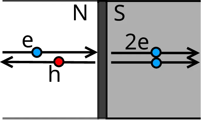
The DC Josephson effect is explained by a process known as Andreev reflection (Schrieffer and Tinkham 1999). A.F.Andreev explained the phenomenon in 1964 establishing the concept of the so-called Andreev reflection This reflection occurs at the interfaces between the superconductor S and a normal metal N. Andreev suggested that an electron that approaches the interface from the normal metal side can travel through the superconductor side by the formation of a Cooper pair with another electron with opposite momentum and spin on the superconductor side. At the same time, reflect a hole inside the normal metal region thus balancing the charge. As a result of this cycle, a pair of correlated electrons is transferred from one superconductor to another, creating a supercurrent flow across the junction. It explains how a normal current in the normal metal side becomes a supercurrent in the superconductor side. The AC Josephson relation in essence suggests that a Josephson junction can be a perfect voltage-to-frequency converter. The inverse is also possible by using a microwave frequency to induce a DC voltage in a Josephson junction, this phenomena is known as inverse AC Josephson effect.
RCSJ model
A Josephson junction, is typically composed of two superconducting electrodes separated by weaklink which is typically insulating, thus such a junction would have some unavoidable capacitance \(C\) (Just like the parallel plate capacitor separated by a dielectric). If the junction current exceeds the critical current of the junction then quasi-particle excitations are generated. These quasi-particle currents are not superconducting and can be quite lossy just like a normal metal current, so we represent this as a normal resistor \(R\). This gives us the resistively and capacitivly shunted junction (RCSJ) model. This model helps us simulate the characteristics of a Josephson junction. A schematic representation of the same can be seen in Fig 1.
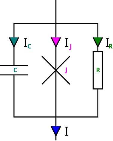
Writing out Kirchov’s circuit laws for the RCSJ model (from Fig 1.)we can find
or
Rearranging as
we can interpret Eq [eq:dammpedeqn] as the dynamics of a damped particle with the following physical properties:
The dynamics of the Josephson junction phase difference in-terms of the damped particle can be described as follows: (Fig 2)
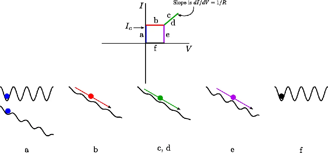
-
When there is no junction current (at I=0) the junction experiences a purely cosine potential. At this stage the pseudo-particle sits trapped in one of the wells of the cosine, as indicated in Fig 2a. As we introduce some current we see the effect of an added linear term to the potential. The potential now resembles a tilted washboard, and hence is called as the tilted washboard potential. If the bias current is less than \(I_{C}\) there are still vallies in the potential and the ball remains trapped as indicated also in Fig 2a. Because the junction phase (i.e the pseudo-particle) is stuck at a fixed value of \(\delta\), the voltage is zero (as \(V\propto\dot{\delta}\) ). This is the part of the IV curve where increase in junction current does not lead to increase in the junction voltage, as indicated in the horizontal blue line. At this stage since the junction element is still superconducting, all of the current flows through the tunnel element and none flows through the resistor thus the junction .
-
As we increase the current past \(I_{c}\), the linear term in the potential dominates the cosine part and the vallies start to disappear. The junction pseudo particle then rolls down hill as shown in Fig 2b. The pseudo particle now experiences a time varying phase, thus the junction voltage becomes non-zero and reaches to a finite value, this can be seen in the red line in Fig 2b
-
Now, the current I exceeds the critical current of the tunnelling element and so the tunnelling element no longer behaves as a superconductor. Quasiparticles are generated, rendering the junction resistive. In other words nearly all of the current flows through the resistive element. Further increases in current show an accompanying linear increase in voltage according to \(V=IR\), similar to that of a normal metal as shown in Fig 2c, and by the green line marked Fig 2c.
-
As the current is lowered, we travel back down the green line, as indicated by the mark Fig 2d. The rest of the process depends on how fast we are raising and lowering the current. As we lower the current below \(I_{c}\), the potential regains its cosine nature and regains vallies.
-
If there were no dissipative forces as is the case when we sweep fast enough or when whatever dissipation remains can’t completely stop the particle, the particle would continue to roll down as it already has energy. Therefore, even as I is lowered below \(I_{c}\) we still have time varying \(\delta\) and therefore still have a measurable voltage. This can be concluded from Fig 2e and the pink line in Fig 2e
-
In the end, we go back to no bias case where the potential is again a cosine term and as we slowly sweep the voltage we slow down and finally stop the particle. Then as we increase the negative bias the process starts all over in reverse.
Josephson Junctions in the Presence of a Magnetic Field
In Eq[eq:JJ1] we saw that he Josephson Junction current depends on the phase difference \(\delta\) across the junction. When an external magnetic field is applied, the field influences the phase difference \(\delta\), this in turn causes interesting dynamics between the Josephson Junction current and the applied external magnetic fields. It can be shown that in the case of a small Josephson Junction this dependence follows the relation(Schrieffer and Tinkham 1999):
here \(\Phi_{J}=\mu_{0}HLd\text{ is the magnetic flux linked to the whole barrier }\). This is the standard from of the Fraunhofer pattern \(F(x)=I_{0}\sin^{2}(\pi x)/(\pi x)^{2}\)and is seen as a unique characteristic confirmation of a Josephson junctions. For a SQUID, the critical current-magnetic field characteristic is similar to that of Josephson Junctions with the addition of SQUID oscillations superimposed on it. Both of these signatures are verified experimentally for the devices fabricated in lab in later sections.
Experimental Details
Sample preparation
For our Josephson junction device we chose the superconductor as Niobium and the weaklink as Copper, based on availability of sputter targets in the lab. These devices were prepared on a 5 x 5 \(mm^{2}\) \(Si/SiO_{2}\) substrate cut from a \(Si/\)\(SiO_{2}\) wafer. The substrates were cleaned with acetone and trichloroethylene both of which are de-greasing agents and IPA which removes any strains left from acetone, followed by DI water bath to remove the residue of the \(SiO_{2}\) or Si on the substrates. Each process was carried out with ultrasonication for 5 minutes in a cleaned beaker. the substrates were then cleaned with the compressed air along with Some IPA in it. The air gun pressure was maintained at 4 PSI. We tried our best to minimise the interface roughness of the sample and to grow the thin-film uniformly.
In order to confirm the presence of magnetic moment in the presence of a SOC material at the weaklink of Josephson Junction and SQUID, we wanted to make Pt/Cu/Nb planar junction ( and SQUID ) where Pt is the bottom layer. We also wanted to observe the effect of varying thickness of the platinum layer and the copper layer. All the samples, thus essentially contain three layers : Nb (155nm), Cu ( varying between 30nm to 100nm), Nb (155nm). For planar Josephson junction the third layer made of Niobium was absent. For all of our requirement we optimized all the thickness of the material before using in trilayer study or making devices. All the instruments apart from the deposition system used in the fabrication process were used inside a clean room.
Lithography
For device fabrication like, planar Josephson junction and planar SQUIDS, we need a 2\(\mu m\) width line made of Nb/Cu/Pt trilayer. For optimizing thickness and do the characterisation for all the layers individually, we did it on same 2\(\mu m\) width track. The patterns were made with the mask aligner lithography machine (Midas MDA-400M) followed by a high precession speed controlled Spin coater.
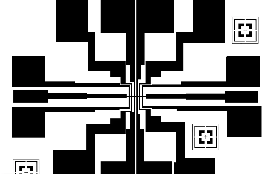
In order to make the 2\(\mu m\), we used photo lithography process with a pre-made mask. The mask contains the 2\(\mu m\) line along with lines drawn on the contact pad at regular intervals. This allows us to make 7 devices at a time on the same sample. An image of the mask is shown in Fig 3.
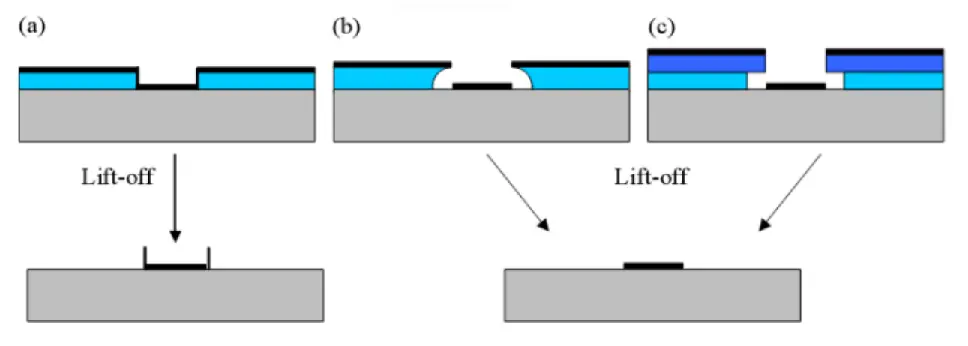
For the photo lithography process, \(Si/\)\(SiO_{2}\)wafer was cut in to several 5mm x 5mm substrate. after cleaning the substrates in the above mentioned process, a uniform layer of ma-N microresist (+ve ) Photoresist was applied to the clean substrates and then spun rapidly using a spin coater at 3000 RPM to even out the photoresist layer, and then baked at 70\(^{\circ}\)C for 1 minute to evaporate the solvent. After the photoresist was applied, the mask was placed on Mask aligner and was exposed to the UV light for 30s to weaken the photoresist on the exposed area. Since these trilayer height were more than 300nm, there were difficulties while doing the liftoff process. The stress on the bottom layer creates an slanted edge on track. So while liftoff there is some possibilities that the 2\(\mu m\) line come out because of the stress from outside photoresist. To avoid these circumstances we used the undercut process in the lithography, the undercut process helps us in making the photoresist edge in a convex shape as shown in Fig5. Which would help us to make a discontinuity in the track height thus easing the liftoff process.
In the case of a positive photoresist, the UV radiation exposed region of the photoresist becomes soluble in the developing solution (Sodium hydroxide solution). After the developing, the photoresist forms a negative image of the required pattern.
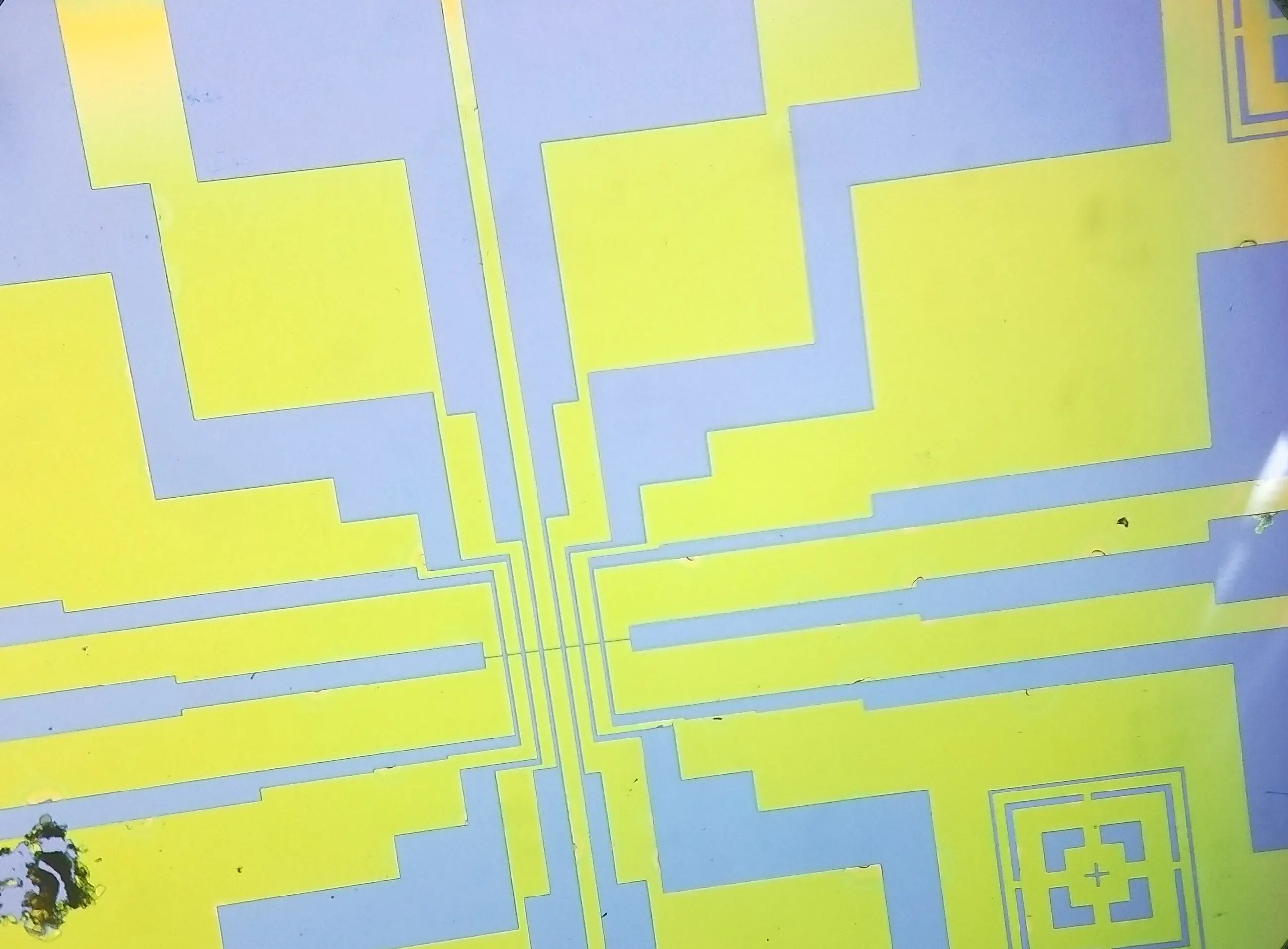
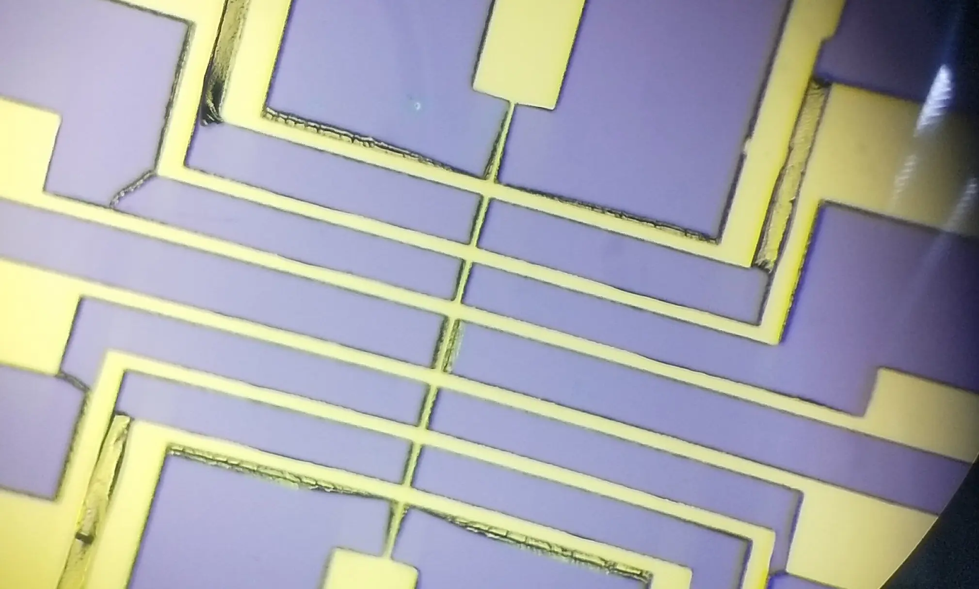
Image taken from optical microscope of the sample after the photolithography process is shown in Fig 6. One can clearly see the part where the photoresist is present (yellowish in colour) and where the photoresist is absent ( due to the \(Si/\)\(SiO_{2}\)substrate below).
During deposition, the material would cover these gaps and upon liftoff the material deposited on the photoresist would go away along with the resist leaving just the material at the desired place as shown in Fig 7.
Deposition
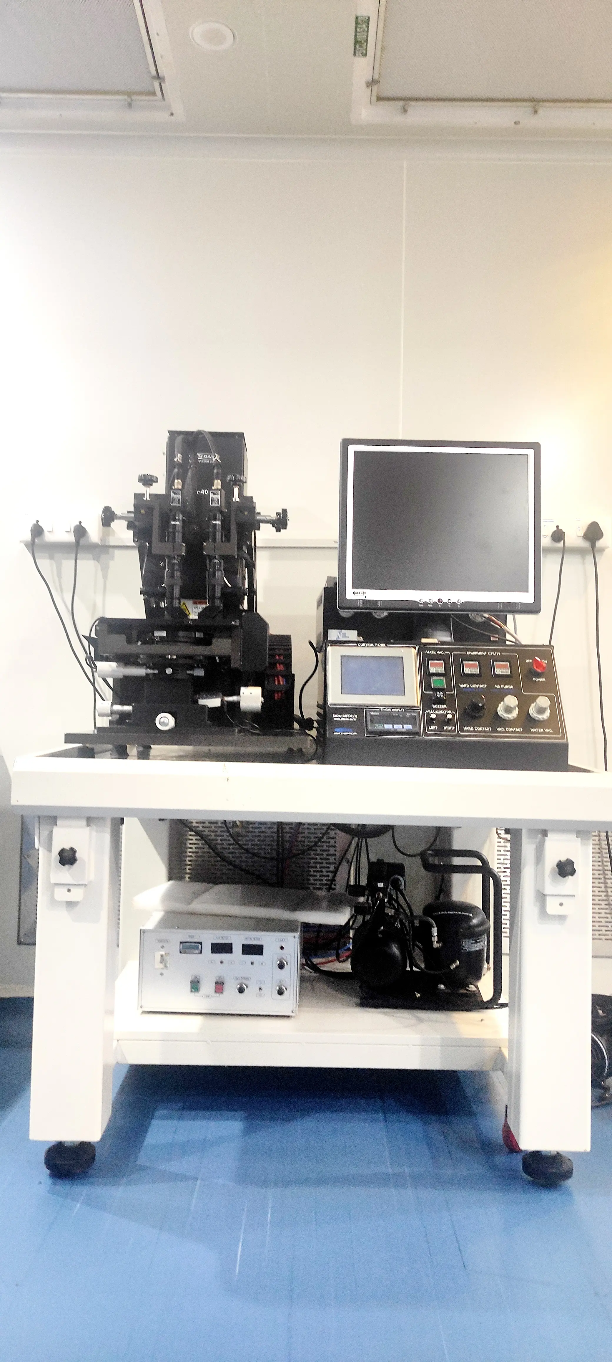
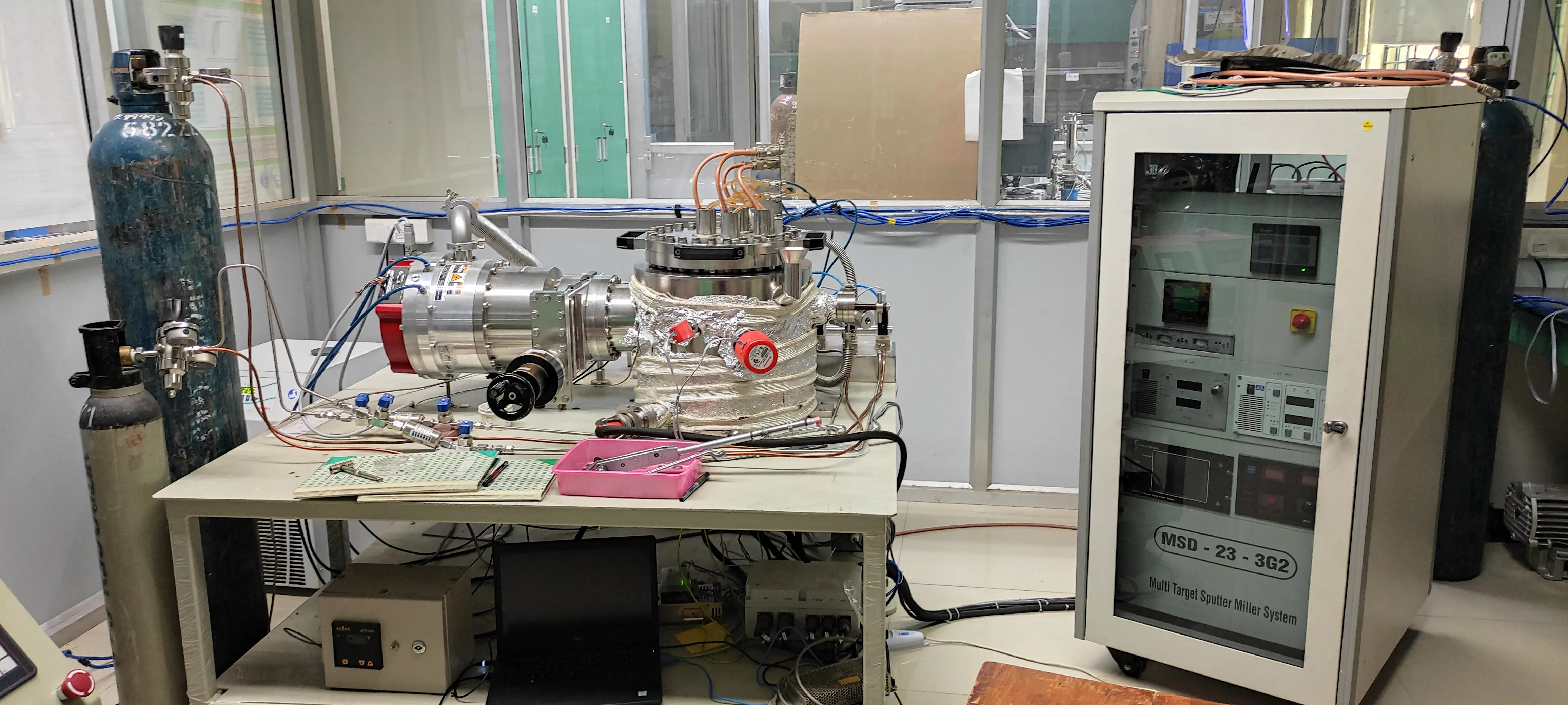
Pt/Cu/Nb trilayer films were prepared on patterned substrates at ambient temperature using DC-magnetron sputtering with high purity (99.99%) Pt,Cu and Nb targets. The DC-magnetron sputtering system present in superconductivity lab, NISER is shown in Fig 8.
The base pressure of the deposition chamber was of the order of \(10^{-9}\)mBar. At normal temperatures standard vacuum chambers have a tendency of holding \(H_{2},H_{2}O\) and CO molecules by physical adsorption at the inner surface of the chamber and could take hours before they are pumped outside. By baking the chamber walls to 150\(^{\circ}\)C for about 12hrs and then cooling the contaminants could be pumped out further. A Residual Gas Analyser (RGA) was used to measure the pressure of contaminants. RGA is a small mass spectrometer typically used for contamination monitoring in vacuum systems. The RGA is able to effectively determines the chemical composition of the residual gas within the vacuum chamber, it works by ionising the residual gases present in the chamber to create ions of these gas molecules before determining their mass-to-charge ratio. It has a working range from \(\approx5\times10^{-2}\) mbar to \(5\times10^{-8}\) mbar.
The typical pressure of \(N_{2},O_{2},H_{2}O\) in \(10^{-8}mBar\) are 3,3,3.5. If the contaminant pressure is more than this base line, Titanium Sublimation pump (TSP) is used as many times as need to obtain the base line. A TSP works by heating a titanium filament wire to about 1300\(^{\circ}\)C by passing about 40A current for a minute. TSP is a type of vacuum pump used to remove residual gases in ultra-high vacuum systems. It has a titanium filament, when a sufficiently high current is passed, the filament reaches the sublimation temperature of titanium and which causes the surrounding walls of the vacuum chamber to gets coated with a layer of clean titanium. Due to the highly reactive nature of titanium, the gas molecules that collides with the titanium coated chamber walls are likely to chemically react with the titanium to form a stable, solid product. Thus reducing the gas pressure in the chamber. Pure Argon was then introduced to the chamber via a mass flow controller at the rate of 20SCCM. The argon helps in initiating the argon plasma across the target. The energetic ions are accelerated towards the target. The ions strike the target and atoms are ejected (or sputtered) from the surface. To initiate plasma generation, high voltage of constant power is applied between the cathode ( located directly behind the sputtering target ) and the anode (which is also connected to the chamber as electrical ground). Electrons which are present in the sputtering gas are accelerated away from the cathode causing collisions with nearby atoms of sputtering gas. These collisions cause an electrostatic repulsion which ‘knock off’ electrons from the sputtering gas atoms, causing ionization. The positively charged sputter gas atoms are now accelerated towards the negatively charged cathode, leading to high energy collisions with the surface of the target. Each of these collisions can cause atoms at the surface of the target to be ejected into the vacuum environment with enough kinetic energy to reach the surface of the substrate. In order to facilitate as many high energy collisions as possible – leading to increased deposition rates – the sputtering gas is typically chosen to be a high molecular weight gas such as argon or xenon. Strong magnets behind the cathode is used to confine the electrons in the plasma at or near the surface of the target. Confining the electrons leads to a higher density plasma and increased deposition rates. The target is cooled by water so that the heat generated will not build up to effect the magnets which keeps the plasma from spreading Shutter plates made of stainless steel is placed in front of target with a narrow opening in order to further improve the deposition. The sample stage is slowly rotated such that the substrates get slowly exposed to the plasma via the shutter plate opening thus enabling even deposition. The height from the substrate plate to the target, the plasma power, the plasma ignition pressure and the argon flow rate are all optimised for each material, previously for good quality deposition. Shutter plate opening width and sample stage rotation speed is optimised for deposition thickness for each target. The following table summarises the various optimisation parameters for the three targets:
| Target | Sputtering pressure | Height of substrate from target | Plasma power | Argon flow rate | Shutter plate opening width | Sample stage rotation speed |
|---|---|---|---|---|---|---|
| Nb | 1.08x10⁻²mbar | 30 mm | 55 W | 20SCCM | 25.2 degree | 0.06 deg/min for 155nm |
| Cu | 1.08x10⁻²mbar | 30 mm | 50 W | 20SCCM | 10.8 degree | 0.1 deg/min for 100nm |
| Pt | 1.08x10⁻²mbar | 30 mm | 50 W | 20SCCM | 10.8 degree | 1 deg/min for 20nm |
Optimisation parameters for different targets
Fabrication geometry
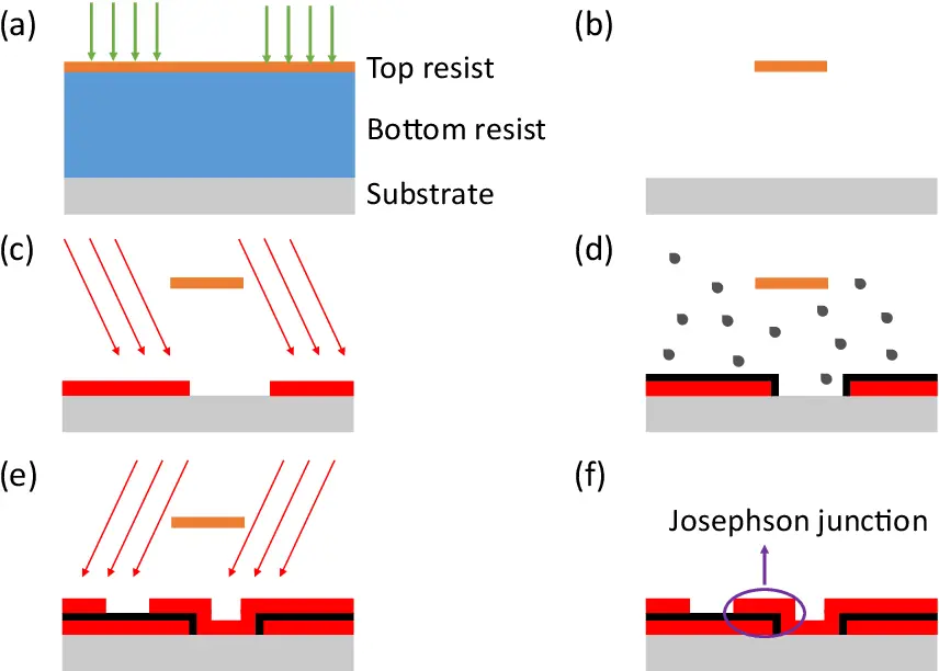
Once the trilayer has been deposited and liftoff is done, we need to form the trilayer into the Josephson junction geometry. Josephson Junctions are typically fabricated via shadow deposition wherein a floating mask and angled deposition creates valleys such that the top and the bottom layers can be accessed separately. After the first angled deposition, controlled oxidation of the first layer leads to the formation of a very small insulating barrier. A schematic process diagram of the shadow deposition technique is shown in Fig 9.
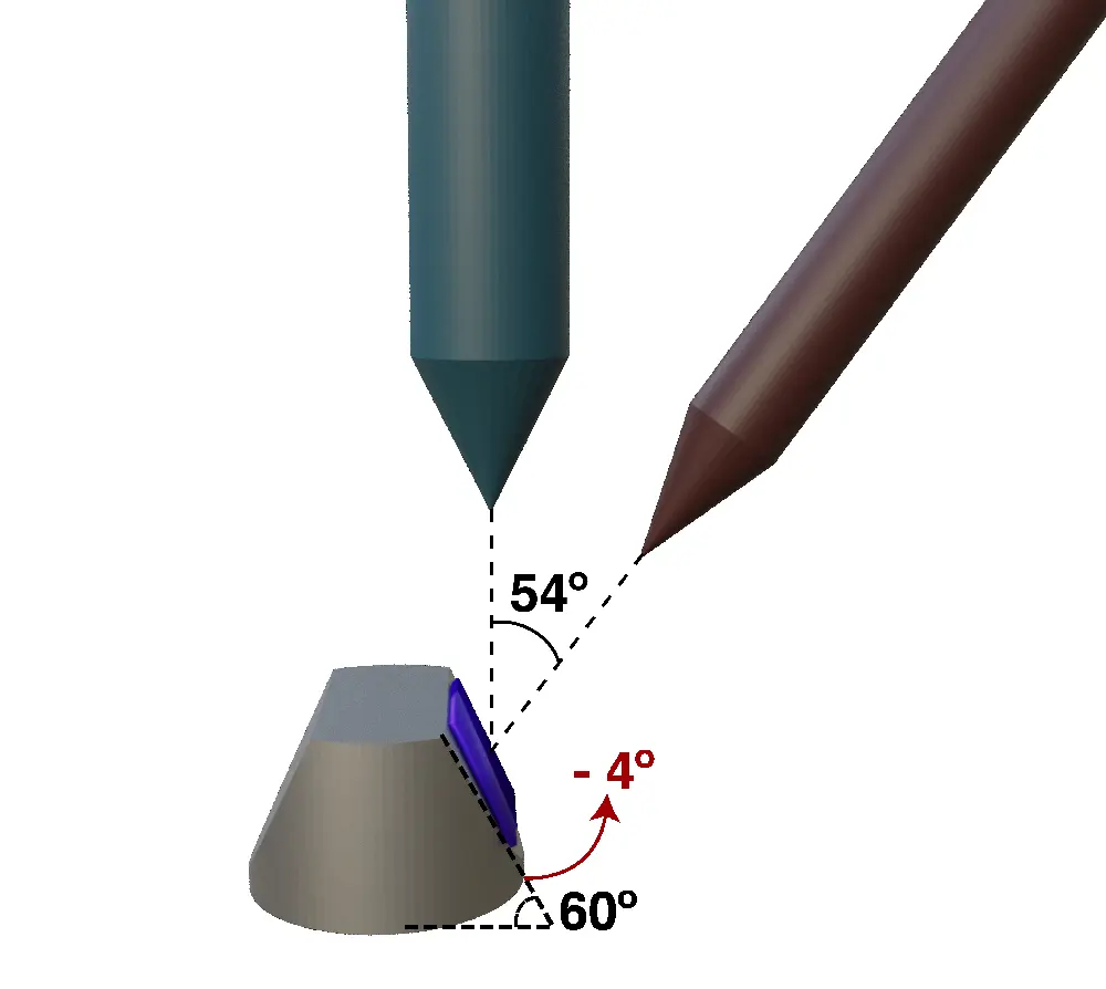
Another way to get to the required geometry is to use a subtractive manufacturing process like a Focused Ion Beam (FIB). A FIB is similar to and SEM in that it uses a beam of ions to image and directly modify or mill the specimen surface via the sputtering process. This milling can be controlled with nanometer precision. Crossbeam 340 from ZEISS, which uses gallium ions for the FIB is available in NISER and was used extensively for the fabrications of the Josephson junction samples. The Crossbeam 340 has a FESEM and gallium FIB guns mounted at \(54^{\circlearrowleft}\) to each other. The sample and the stage is adjusted such that the focal axis of both FIB and SEM co-inside at the surface of the sample and is at a working distance of 5.12mm away from the gun tip. This alignment shown in Fig 10 ensures that the imaging done by the SEM and the milling done by the FIB co-inside.
While milling, highly energised gallium ions strike the sample causing the target to sputter atoms from the surface. In this process gallium atoms will get embedded in the top few nano meters of the target surface, and the surface will become amorphous, this is known as gallium poisoning.
There are two geometries in which the Josephson junction are fabricated using FIB, one is the vertical Junction (Fig 12), and the other is the planar Junction (Fig 11); both names describe the path the current takes through the trilayers. In the planar Junction, the current is in plane with the trilayers and in the case of the vertical junctions the current flows vertically through the trilayers.
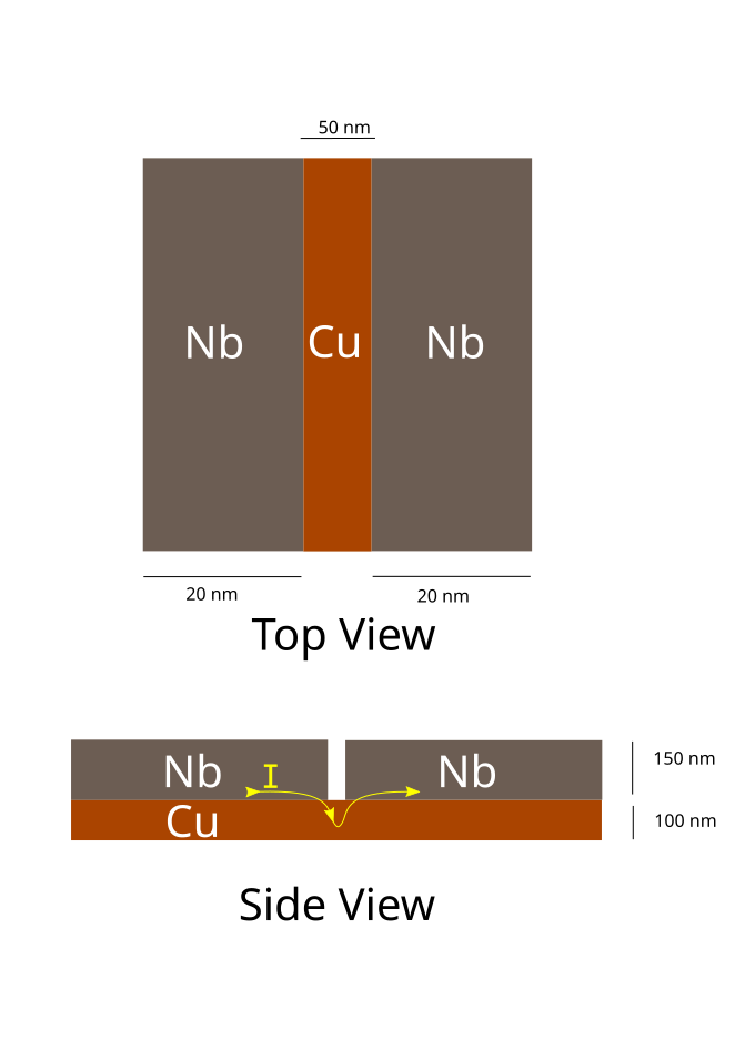
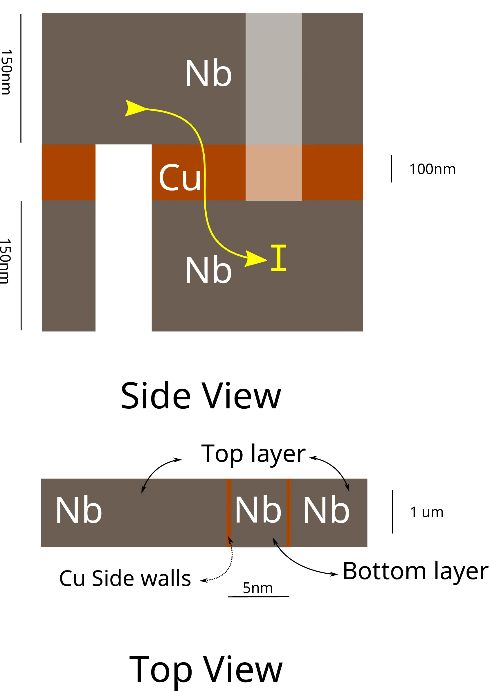
In order to do the Planar, cut the stage was tilted in such a way that the sample is perpendicular to the FIB gun, similar to the arrangement in Fig 10. Then a vertical cut is made to a controlled depth.In order to control the depth of the cut, exposure time had to be optimised. This was done by cutting several vertical lines away from the 2\(\mu\) line with varying exposure time. Then Energy Dispersive Spectroscopy (EDAX) was done on these multiple cuts to see which exposure time first cuts the Niobium layer and thus exposing the Copper below it (Fig 13).
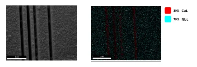
The basic principle of EDAX is as follows: During SEM microscopy, the primary electron beam sometimes removes electrons from the inner shells of an atom causing the outer electron to jump into the vacant spot by releasing energy in the form of X-rays. This energy difference is unique for each element and the element can be identified from it’s characteristic X-ray. EDS measures these characteristic X-rays thus identifying the chemical composition of the sample.
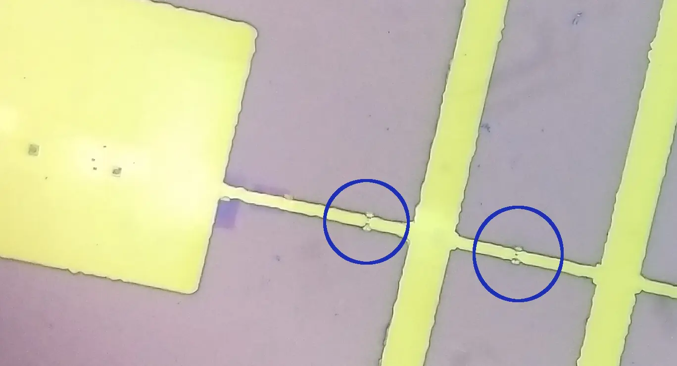
An image of the sample after milling with FIB as seen through an optical microscope is shown in Fig .
Wire bonding
After the sample is prepared, electrical connections need to be made for sending current, measuring voltage,etc. For this a wire bonding apparatus is used which uses 50\(\mu m\) dia silicon doped aluminium wires for the connections. The needle through which the aluminium wire comes through, embeds the wire in the sample by vibrating at ultrasonic frequencies.
Ultrasonic bonding was discovered 1960 through a several experimental observation and has subsequently been developed into a highly controlled process. In recent years it has been used extensively for electrical interconnecting of semiconductor chips in the semiconductor fabrication industry and in material science research laboratories for making reliable conducting contacts on sample and pucks. There are four types of wire bonding:
Thermocompression Bonding A process which involves the use of force, time, and heat to join the two materials by inter- diffusion. This process uses gold wire.
Gold Ball Bonding Uses gold wire ultrasonicated at the surface to make the ball. This process uses heat force, time, and ultrasonics.
Wedge Bonding This process uses aluminium wire formed below a narrow metalic wedge. The wedge forces the wire on top of the sample and ultrasonicates therby making a metallic bond between aluminium and the sample. No heat is required in this process. This process is the one used all the sample preparation in regards to the current thesis.
Thermosonic Bonding This requires gold wire and capillaries. This process uses force, time. heat, and ultrasonics to make a ball. This process is accomplished by melting the wire to form a ball.
Wedge Bonding
Ultrasonic energy, when applied to metallic wire to be bonded, renders it temporarily soft and plastic. This causes the metal to flow under pressure. The acoustic energy frees the dislocation from their pinned positions which allows the metal to flow under the low compressive forces of the bond. Thus heat at the bond becomes a byproduct of the bonding process, and the heat becomes unnecessary to form the bond. The deformation of the wire will break up and sweep aside the contaminants in the weld area. This exposes extremely clean metallic surfaces which promotes the metallurgical bonds.
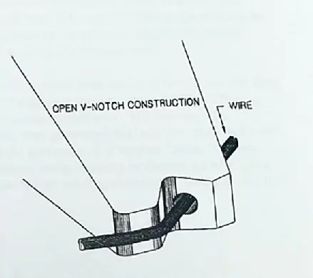
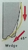
In wedge bonding, the wire come out through a 50 \(\mu m\) hole at 45° angle and then under the needle tip which is shaped like a wedge as seen in Fig [fig:Image-of-wire].
The quality of wire bonded is also sensitive to the height between the base plate and the needle tip when it is bonding, the wirebonder at NISER is setup such that this effective height is 76mm, at this height ultrasonic power and the bonding force are most effective, because the transducer is in surface and the bond tool stands perfectly vertical. Therefore the distance from base plate should always be fixed to this value.
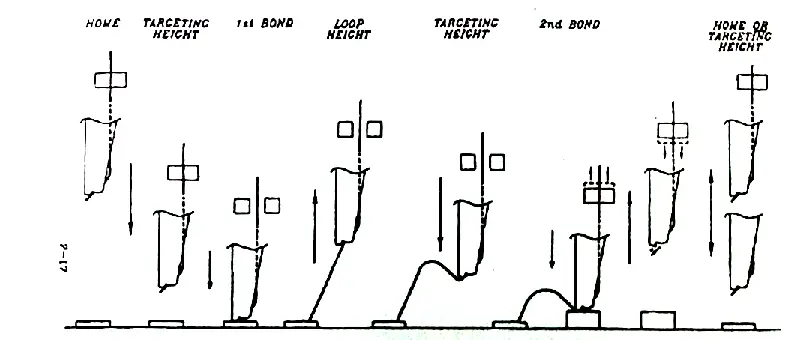
In case the Surface is higher, the bond will be affected when the tool touches the surface. At a surface height >78 mm the ultrasonic power and bonding force are less effective and most probably the parameters have to be increased. If the bonding surface is lower than 76 mm, the bond will be automatically activated at a height of 75.5 mm, even if the tool does not touch the surface. So it is impossible to bond at a lower height. The steps involved in making the two bonds are shown in Fig 15.
A principle disadvantage of wedge bonding is the wire is fed at a 45° or 60° horizontal angle rather than perpendicular as in ball bonding. Also, wedge bonding is unidirectional.
This is slower than ball bonding which is multidirectional. Wedge bonding requires the circuit workpiece or the bonding head to rotate to allow for the wire to bond in the appropriate direction.
Characterization
Physical Property Measurement System (PPMS)
In order to do analysis/characterisation of any material/nano device, one typically need measurement of several physical properties of DUT. Typical physical characteristics like,
-
Resistance as a function of temperature
-
Current voltage characteristics
-
Magnetic susceptibility as a function of applied external magnetic field (VSM)
-
Magnetoresistance
-
Other transport measurements like specific heat, magnetic AC and DC susceptibility and both electrical and thermal transport properties (like Hall Effect, thermoelectric figure of merit and Seebeck Effect) etc.
are most often used to characterise bulk and thinfilm samples. Superconductivity lab, NISER has a PPMS setup by Cryogenics that allows one to do low temperature characterisation of materials (1.6K - 300K) at different magnetic fields (upto 9 Tesla) and under different electric configuration of the sample. Fig17 shows the image of the PPMS system present in the lab.
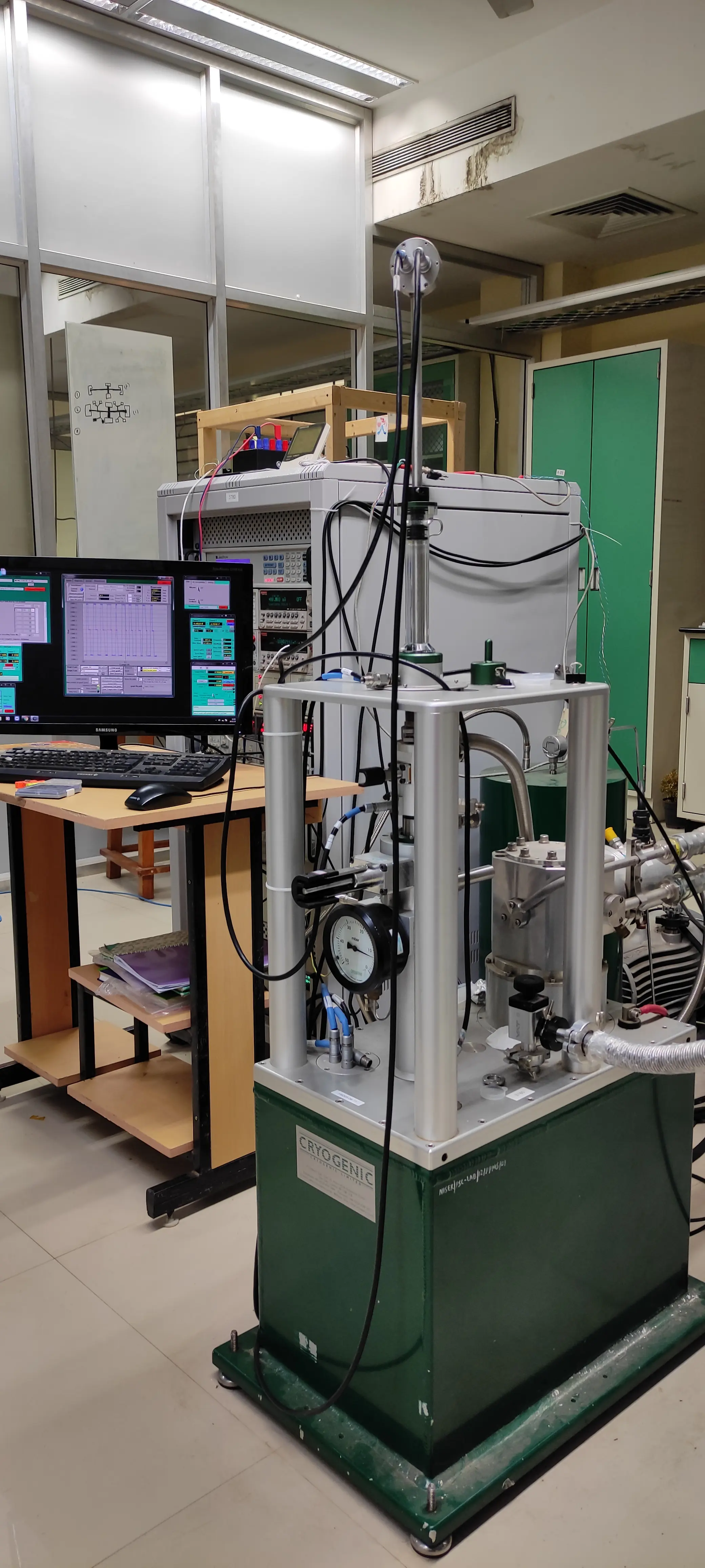
The setup comprises of the following main components:
-
A cryostat incorporating a cryocooler, superconducting magnet and a variable temperature sample space.
-
Rack incorporating electronics for control and monitoring of the cryostat and any measurement options.
-
Measurement system software for control of measurement instruments from a computer
-
Sample probes for various measurement configuration (Transport measurement,a probe for vibrating sample magnetometer and a rotating stage for transport measurement).
Cryocooler
Cooling materials to such a low temperatures has traditionally used liquid cryogens (usually helium and nitrogen). The samples were essentially dipped in a dewar containg liquid Helium/Nitrogen. On the other hand cryocooler operate using a helium compressor, makes use of adiabatic expansion of these liquids to reach temperatures below the boiling point of these cryogens.
There are two types of cryocooler that are typically used, the Gifford McMahon (GM) cryocooler and the Pulse Tube (PT) cryocooler. The PPMS in our lab uses Pulse Tube type cryocooler. The GM cryocooler has the advantage of greater thermodynamic efficiency and reliable operation in any orientation.The PT cooler has no cold moving parts so is quieter and has longer service intervals. The PPMS has two cooling stages. The first one is through the circulation of compressed helium via the compressor and the second stage is via adiabatic expansion of the liquid helium stored in a He pot. The first stage produces about 50W of cooling power at about 40K and the second stage provides about 1.5W of cooling power. The second stage cools the sample space and the cryogenic superconducting magnets. The flow of the helium throught the close cycle can be understood interms of the following steps. Helium gas is stored at room temperature in a Helium dump vessel. An oil-free pump drives the circulation of the helium gas into the VTI circuit from the He dump. The gas first passes through a charcoal filter which removes any impurities within the gas. It then flows through the first stage heat exchanger which cools the gas to 40K. The gas then passes to the second stage of the Cryocooler where it is cooled further to below 4 K and condenses in the helium pot. The helium then flows across the needle valve, after which it expands and cools further to approximately 1.6K. It then travels through the VTI heat exchanger where the helium is warmed as necessary. Helium gas then flows up past the sample to the top of the VTI where it exits and travels back to the pump and dump. The sample space temperature is controlled by the cooling action of the helium and the heating action of the heater present in VTI. A PID controller is used to precisely reach any given set point. The cooling capacity of the system depends on the vapour pressure of the helium throught the needle valve thus careful adjustment of needle valve pressure is needed to maintain stable cooling. If the pressure is too low, the system will not cool to the lowest stable state and if the pressure is set too high the cooling power and the heater power would compete with each other thus rendering the system unstable. A pressure of 5-15 mbar is recommended by the manufacturer. However, if the flow rate is far too high, the amount of heat that needs to be extracted from the circulating helium exceeds the cooling power. So, the temperature of the 2nd stage, magnet and helium pot will increase which is bad for the system.
Superconducting Magnets
There two superconducting magnets in the system, one for low field (upto 25mT) and the other for high field. The magnet is a vertically oriented solenoid wound on niobium titanium (NbTi) superconducting wire. NbTi is specifically chosen because of its hight current carrying capacity before becoming normal. The coil is cooled by the cryocooler to an operating temperature of 3 — 4 K. If the temperature exceeds this range then what we call as quenching can happen, which is where a part of the coil becomes normal increasing the resistance considerably, thereby dissipating the energy flowing in the coil as heat which in turn propagates the normal region. This happens until the entire coil becomes normal and might cause degradation to the coil.
DC Resistivity Probe
In order to verify that the sputtering parameters yielded the expected thickness of the trilayers, a line was drawn on the substrate with a marker before deposition, and post-deposition washing the substrate with IPA introduced a cut in the sample that was then analysed with a contact step profilometer. The profilometer data agreed with the expected thickness.
Prior to making the devices, magneto-transport measurements of the trilayer above the critical temperature of Niobium showed no hysteretic signature, nor was any anomaly in the magnetoresistance observed. The trilayer also had a sharp superconducting transition (due to the Niobium layer) at 6-7 K indicating a good quality deposition.
Results
Measurements
All the superconducting devices were first cooled to sub 2K, and then a 4 probe resistance vs temperature measurement was carried out with 1 - 10 \(\mu\)A by ramping the temperature slowly to 10K, in order to see the phase transitions. One such R-T graph is shown in Fig 18.
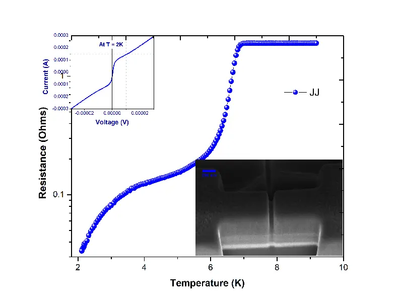
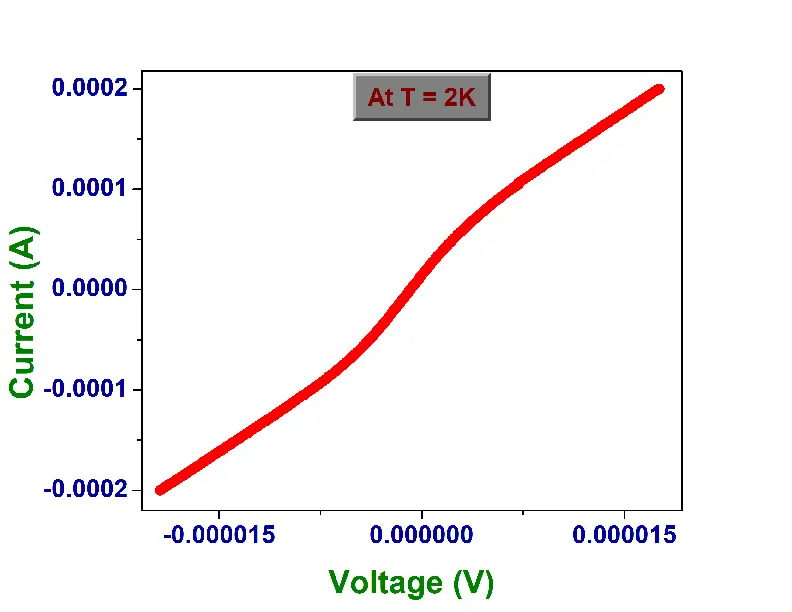
The first transition indicates the superconducting transition of the Niobium layer, and the second transition explains the proximitisation of the weak link. The resistance \(R_{n}\) at 9K (above \(T_{c}\)) and \(R_{L}\)at 2K are noted and the sample is cooled back to sub 2K. \(R_{n}\)is the normal resistance and indicates that the device is out of the superconducting regime. Once the devices cool down to 2K the current-voltage characteristics of the device is measured by sweeping current from -\(I_{n}\) to +\(I_{n}\), where \(I_{n}\) is the current for which the device yields the resistance \(R_{n}\) at 2K, ie. the device switches to the normal regime. The I-V curves have the typical JJ/SQUID behaviour and is plotted in Fig 19.
\(I_{c}\) of the device and the electrodes were extracted from this data by running through a python script that takes in the I-V data, calculates dV/dI, and applies a Savitzky–Golay filter of first-order to obtain \(d^{2}I/d^{2}V\) and find the current (\(I_{c}\)) for which \(d^{2}I/d^{2}V\) in both the positive and negative side and averages them. For normal Josephson junction the position of peak of \(dI/dV\) is a good marker of the \(I_{c}\), however in cases where the junction resistance is high, \(dI/dV\) might not be clear enough to mitigate this peaks of \(d^{2}I/d^{2}V\) is a better marker of \(I_{c}\) A sample graph of \(dI/dV\) and \(d^{2}I/d^{2}V\) for a I vs V curve measured on a Josephson junction is shown in Fig 20.
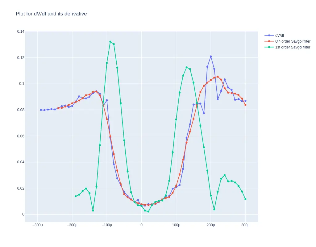
The code for the python script is available here and a web app based on the same is hosted at jj-ic-finder.streamlit.app
In Fig 19 the IV curve of a Nb/Cu Josephson Junction is shown. Once the device \(I_{c}\) is found, the device is cooled to 2K and then supplied with \(I_{c}\) current, and the junction voltage is measured while ramping the magnetic field from +250 Oe to -250 Oe ( positive cycle ) and then from -250Oe to 250Oe ( negative cycle ) at 2K. This gives us magnetoresistance as a function of the applied magnetic field. The magnetoresistance as a function of applied magnetic field is expected to have a diffraction pattern for JJs and SQUID oscillations imposed on top of the diffraction pattern for SQUID device as can be seen in Fig 21 and Fig 22. This was explained in the theoretical sections above.
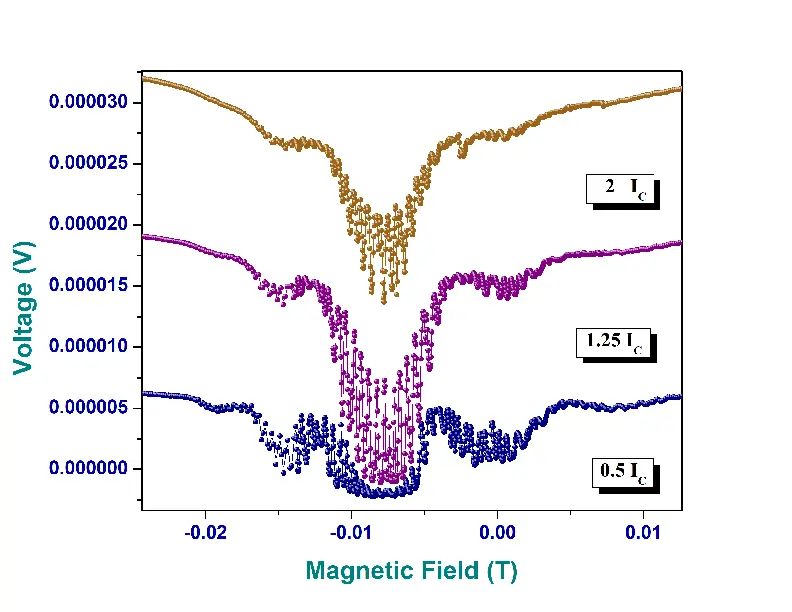
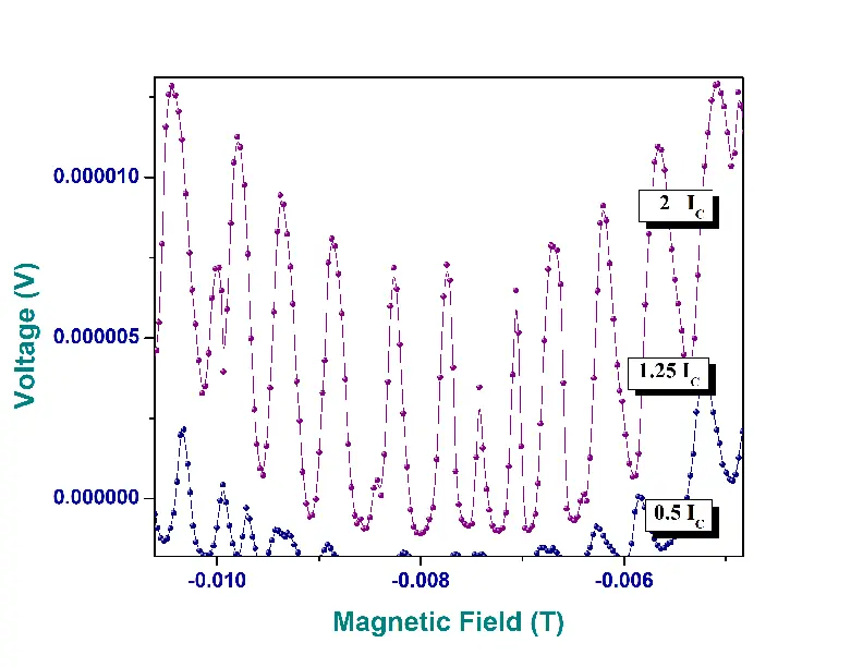
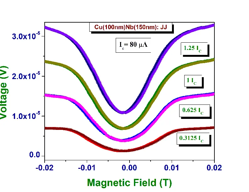
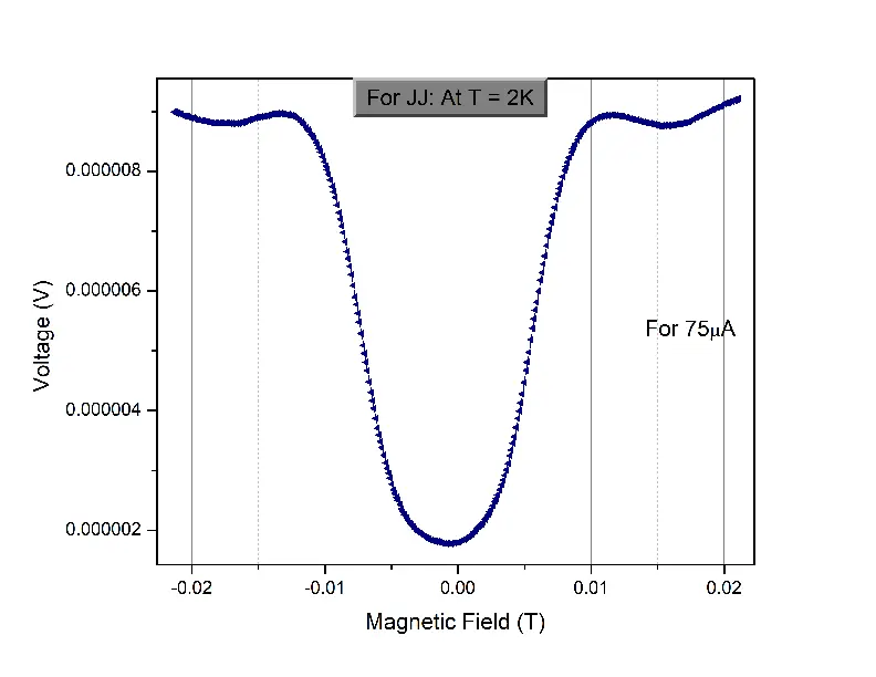
In Fig 24 , we examine the magnetoresistance of the patterned Nb/Cu Josephson junction device in low magnetic fields (|H| < 300 Oe) and at its \(I_{c}\). We find that the main lobe of the positive and the negative cycle overlap completely and there is no shift of the main lobe from origin as one would expect for a normal S-N-S junction. Fig 23 is a plot of Junction voltage as a function of magnetic field for another patterned Nb/Cu Josephson junction device in low magnetic fields for different values of junction currents. Once can observe that higher currents increase the height of the lobes however the ratio of the first (main) lobe to the second lobe remains constant.
Discussion and Conclusion
We were able to successfully fabricate vertical and planar Nb/Cu Josephson junctions and through its R-T, I-V, V-H signatures verified that the device works as expected. The R-T graph shoved the superconducting transition of the Niobium electrodes sub 7K and slow proximitisation of the weaklink thereafter. The I-V graph clearly shows the presence of a critical current \(I_{c}\) beyond which the junction behaves resistively, the \(I_{c}\) extraction was automated by analysing the second derivative of voltage with respect to applied current via a python script. The VH graph for Josephson junctions shows clear Fraunhofer like pattern and SQUID oscillations on top of Fraunhofer in the case of SQUIDs thus further confirming the quality of device thus formed. Future direction of the project would be to explore alternative materials for the weaklink of the Josephson junctions. Preliminary literature survey suggest that 0–\(\pi\) oscillations in Superconductor/Ferromagnet/Superconductor junctions with varying thickness of Ferromagnet layer(Stoutimore et al. 2018). \(\phi\) Josephson junctions are seen with topological insulator \(Bi_{2}Se_{3}\) (Assouline et al. 2019)or 2DEG formed at the surface of InAs layer(Strambini et al., n.d.). \(\phi\) junctions are also observed in weaklinks with high spin orbit coupling. Further studies on the properties of such weaklinks might be carried out.
References
Assouline, Alexandre, Cheryl Feuillet-Palma, Nicolas Bergeal, Tianzhen Zhang, Alireza Mottaghizadeh, Alexandre Zimmers, Emmanuel Lhuillier, et al. 2019. “Spin-Orbit Induced Phase-Shift in Bi2Se3 Josephson Junctions.” Nature Communications 2019 10:1 10 (January): 1–8. https://doi.org/10.1038/s41467-018-08022-y.
Bardeen, J., L. N. Cooper, and J. R. Schrieffer. 1957. “Theory of Superconductivity.” Phys. Rev. 108 (December): 1175–1204. https://doi.org/10.1103/PhysRev.108.1175.
DanielSank. n.d. “What Does the \(I\)-\(V\) Curve in Josephson Junction Mean?” Physics Stack Exchange. https://physics.stackexchange.com/q/197150.
Drozdov, A. P., M. I. Eremets, I. A. Troyan, V. Ksenofontov, and S. I. Shylin. 2015. “Conventional Superconductivity at 203 Kelvin at High Pressures in the Sulfur Hydride System.” Nature 525 (7567): 73–76. https://doi.org/10.1038/nature14964.
Josephson, B. D. 1962. “Possible New Effects in Superconductive Tunnelling.” Physics Letters 1 (7): 251–53. https://doi.org/10.1016/0031-9163(62)91369-0.
Klenov, N, V Kornev, A Vedyayev, N Ryzhanova, N Pugach, and T Rumyantseva. 2008. “Examination of Logic Operations with Silent Phase Qubit.” Journal of Physics: Conference Series 97 (February): 012037. https://doi.org/10.1088/1742-6596/97/1/012037.
Lee, Gil-Ho, and Hu-Jong Lee. 2018. “Proximity Coupling in Superconductor-Graphene Heterostructures.” Reports on Progress in Physics 81 (5): 056502. https://doi.org/10.1088/1361-6633/aaafe1.
Ngo, Duc-The. 2021. “Lorentz TEM Characterisation of Magnetic and Physical Structure of Nanostructure Magnetic Thin Films,” December.
Schrieffer, J. R., and M. Tinkham. 1999. “Superconductivity.” Rev. Mod. Phys. 71 (March): S313–17. https://doi.org/10.1103/RevModPhys.71.S313.
Stoutimore, M J A, A N Rossolenko, V V Bolginov, V A Oboznov, A Y Rusanov, D S Baranov, N Pugach, S M Frolov, V V Ryazanov, and D J Van Harlingen. 2018. “Second-Harmonic Current-Phase Relation in Josephson Junctions with Ferromagnetic Barriers.”
Strambini, Elia, Andrea Iorio, Ofelia Durante, Roberta Citro, Cristina Sanz-Fernández, Claudio Guarcello, Ilya V Tokatly, et al. n.d. “A Josephson Phase Battery.” Nature Nanotechnology. https://doi.org/10.1038/s41565-020-0712-7.
TPT. n.d. “HB-05 TPT Wire Bonder Manual.” In.
Wang, Lujun. 2015. “Fabrication Stability of Josephson Junctions for Superconducting Qubits.” In.
Yamashita, T., K. Tanikawa, S. Takahashi, and S. Maekawa. 2005. “Superconducting \(\ensuremath{\pi}\) Qubit with a Ferromagnetic Josephson Junction.” Phys. Rev. Lett. 95 (August): 097001. https://doi.org/10.1103/PhysRevLett.95.097001.
Acknowledgements
I wish to thank my project supervisors, Dr. Kartikeswar Senapati and Dr. Ram Shanker Patel for their immense support and help with the understanding of this project. I would like to express my deepest appreciation to Mr. Tapas Ranjan Senapati and Ms. Laxmipriya Nanda for all their help from mentoring on the fabrication techniques to usage of measurement systems and all the fruitful discussions. I wish to thank all the lab members of Superconductivity lab, NISER for all the brainstorming sessions which helped me greatly. Special thanks to Ms. Soheli Mukherjee who always supported me with all my endeavours. I would also like to extend my deepest gratitude to Dr. Dhavala Suri who always showered me with helpful advice. lastly, I am thankful to all my friends and family members for extending their love and support.
Abbreviations
-
AC :- Alternating current
-
RF :- Radio frequency
-
JJ :- Josephson Junction
-
SQUID :- Superconducting QUantum Interference Device
-
EDX :- Energy Dispersive X-ray spectroscopy
-
SEM :- Scanning Electron Microscope
-
FIB :- Focused Ion Beam
-
PPMS :- Physical Properties Measurement System
-
Fig :- Figure
-
eV :- Electron Volt
-
KeV :- Kilo Electron Volt
-
MeV :- Mega/Million Electron Volt
-
et al :- And others (Latin)
-
i.e. :- That is
-
etc :- Et cetera (Latin for ’and others of same kind’)
-
T :- Tesla
-
SiO2:- Silicon dioxide
-
R-T :- Resistance Versus Temperature
-
I-V :- Current Versus Voltage
-
I-H :- Current Versus Magnetic field
-
V-H :- Voltage Versus Magnetic field
-
Si :- Silicon
-
K :- kelvin
-
mm :- millimeter
-
mbar :- millibar
-
IPA :- Isopropyl alcohol
-
RPM :- Revolutions Per Minute
-
C :- Celsius
-
Ar :- Argon
-
e.g. :- Example given
-
TSP :- Titanium Sublimation Pump
-
RGA :- Residual Gas Analyzers
-
Cu :- Copper
-
BCS :- Bardeen–Cooper–Schrieffer
-
Nb :- Niobium
-
DC :- Direct current
-
AC :- Alternating current
-
\(\mu\)A :- Micro Ampere
-
\(\Omega\):- Ohm
-
nm :- Nano meter